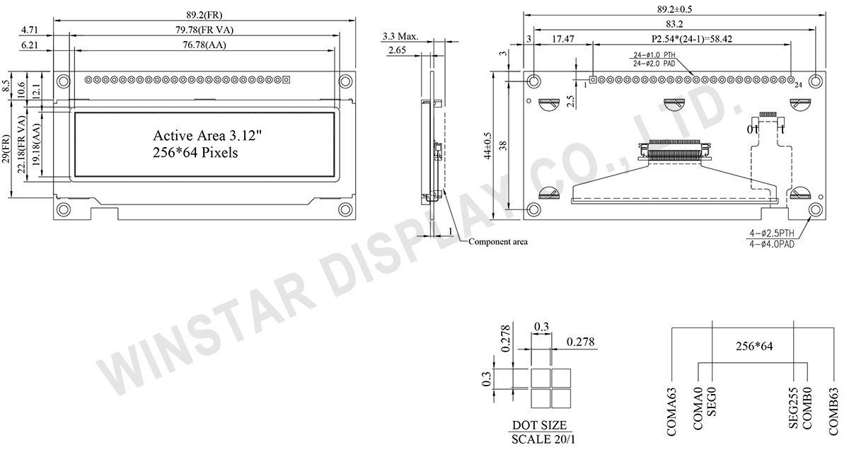
Startseite Produkte OLED-Anzeige Grafik-OLED-Anzeigen WEN025664B

3,12 zoll COF OLED-Anzeigen 256x64 +PCB +Frame

Modellnummer WEN025664B

►Typ: Grafik
►Bauweise: COF+PCB+Frame
►Größe: 3,12" OLED
►256 x 64 Punktmatrix
►Integrierter Controller SSD1322
►3-V-Stromversorgung
►1/64 duty
►Schnittstelle: 6800, 8080, SPI
►die Farbe des Displays: Weiß / Gelb / Himmelblau / Grün
►Support Grayscale

Beschreibung

Das Modell WEN025664B ist ein COF Graphic OLED mit einer Diagonale von 3,12 Zoll und einer Auflösung von 256x64 Pixel. Dieses OLED-Modul ist mit dem SSD1322 IC ausgestattet und unterstützt 8-Bit-6800/8080- sowie 3/4-Leitungs-SPI-Schnittstellen. Es hat eine Außenabmessung von 89,2 × 44,0 mm und eine aktive Fläche von 76,78 × 19,18 mm. Es unterstützt auch 4-Bit- Graustufen, mit einer logischen Versorgungsspannung von 3V. Der Strom des Displays bei 50% auf der Platine beträgt 150 mA @3,0V VDD (typischer Wert), bei einer Treiberpflicht von 1/64.

Das Modul verfügt über eine eingebaute Leiterplatte (PCB), die es Kunden ermöglicht, Drahtverbindungen ohne zusätzliche PCB-Entwicklung für ihre Anwendungen zu nutzen. Darüber hinaus vereinfacht der integrierte VCC-Schaltkreis auf der PCB die Nutzung durch Kunden. Diese Leiterplatte (PCB), ausgestattet mit vier Montagelöchern, bietet Kunden eine einfache Möglichkeit, Module in ihren Anwendungen zu befestigen. Dieses OLED-Modul eignet sich für Anwendungen im Smart Home, in medizinischen Geräten, der industriellen Steuerung, usw.

Das Modell WEN025664B kann in einem Temperaturbereich von -40℃ bis +80℃ betrieben werden, mit Lagerungstemperaturen von -40℃ bis +85℃. Das OLED-Modul zeichnet sich durch ein hohes Kontrastverhältnis von 10.000:1 aus, was zu einer verbesserten Bildqualität, schärferen Details und verbesserter Lesbarkeit, insbesondere bei schwachem Licht, führt.

Darüber hinaus bieten OLED-Panels mit denselben Abmessungen verschiedene Alternativen:

Zeichnung

3.12 inch 256x64 COF OLED Display With PCB and Frame - WEN025664B

Data source ref: WEN025664BWAP3N0000

Technische Daten

Schnittstelle Pin-Funktion

Pin
Number
Symbol I/O Beschreibung
1 VSS P Ground.
2 VDD P Power Supply for Core Logic Circuit
Power supply pin for core logic operation. A capacitor is required to connect between this pin and VSS
3 N.C. P Reserved Pin
The N.C. pin between function pins are reserved for compatible and flexible design.
4 D/C# I Data/Command Control
This pin is Data/Command control pin connecting to the MCU.
When the pin is pulled HIGH, the content at D[7:0] will be interpreted as data.
When the pin is pulled LOW, the content at D[7:0] will be interpreted as command.
5 R/W#
(WR#)
I Read/Write Select or Write
This pin is MCU interface input. When interfacing to a 68XX-series microprocessor, this pin will be used as Read/Write (R/W#) selection input. Pull this pin to “High” for read mode and pull it to “Low” for write mode.
When 80XX interface mode is selected, this pin will be the Write (WR#) input. Data write operation is initiated when this pin is pulled low and the CS# is pulled low.
When serial mode is selected, this pin must be connected to VSS.
6 E/RD# I Read/Write Enable or Read
This pin is MCU interface input.
When interfacing to a 68XX-series microprocessor, this pin will be used as the Enable (E) signal. Read/write operation is initiated when this pin is pulled high and the CS# is pulled low.
When connecting to an 80XX-microprocessor, this pin receives the Read (RD#) signal. Data read operation is initiated when this pin is pulled low and CS# is pulled low.
When serial mode is selected, this pin must be connected to VSS.
7~14 DB0 I/O Host Data Input/Output Bus
These pins are 8-bit bi-directional data bus to be connected to the microprocessor’s data bus.
When serial mode is selected, DB1 will be the serial data input SDIN and DB0 will be the serial clock input SCLK.
DB1
DB2
DB3
DB4
DB5
DB6
DB7
15 NC P Reserved Pin
The N.C. pin between function pins are reserved for compatible and flexible design.
16 RES# I This pin is reset signal input.
When the pin is pulled LOW, initialization of the chip is executed.
Keep this pin pull HIGH during normal operation.
17 CS# I Data/Command Control
This pin is the chip select input connecting to the MCU. The chip is enabled for MCU communication only when CS# is pulled LOW.

18
NC P Reserved Pin
The N.C. pin between function pins are reserved for compatible and flexible design.
19 BS1 I Communicating Protocol Select
These pins are MCU interface selection input. See the following table:
BS:[1:0] Bus Interface Selection
00 4 line SPI
01 3 line SPI
10 8-bit 8080 parallel
11 8-bit 6800 parallel
Note
(1) 0 is connected to VSS
(2) 1 is connected to VDD
20 BS0
21~24 NC P Reserved Pin
The N.C. pin between function pins are reserved for compatible and flexible design.

mechanische Daten

Artikel Ausmaß Einheit
Punktmatrix 256 x 64 Dots
Abmaße der modul 89,2 × 44,0 × 3,3 Max. mm
Aktiver Bereich 76,78 × 19,18 mm
Punktgröße 0,278 × 0,278 mm
Punktabstand 0,3×0,3 mm
der Anzeigemodus Passive Matrix
die Farbe des Displays Monochromes
Drive Duty 1/64 Duty
Gray Scale 4 bits
IC SSD1322 (COF)
Schnittstelle 6800, 8080, SPI
Größe 3,12 Zoll

Absolute Grenzwerte

Parameter Symbol Mindestwert Maximalwert Einheit
Supply Voltage for Display VDD -0.3 4 V
Betriebstemperatur TOP -40 80 °C
Lagertemperatur TSTG -40 85 °C

elektronische Eingenschaften

Artikel Symbol Bedingung Mindestwert typischer Wert Maximalwert Einheit
Supply Voltage for Logic VDD 2.8 3.0 3.3 V
High Level Input VIH 0.8×VDD VDD V
Low Level Input VIL 0 0.2×VDD V
High Level Output VOH 0.9×VDD VDD V
Low Level Output VOL 0 0.1×VDD V
50% Check Board operating Current IDD VCC =3V 150 300 mA
go top
close