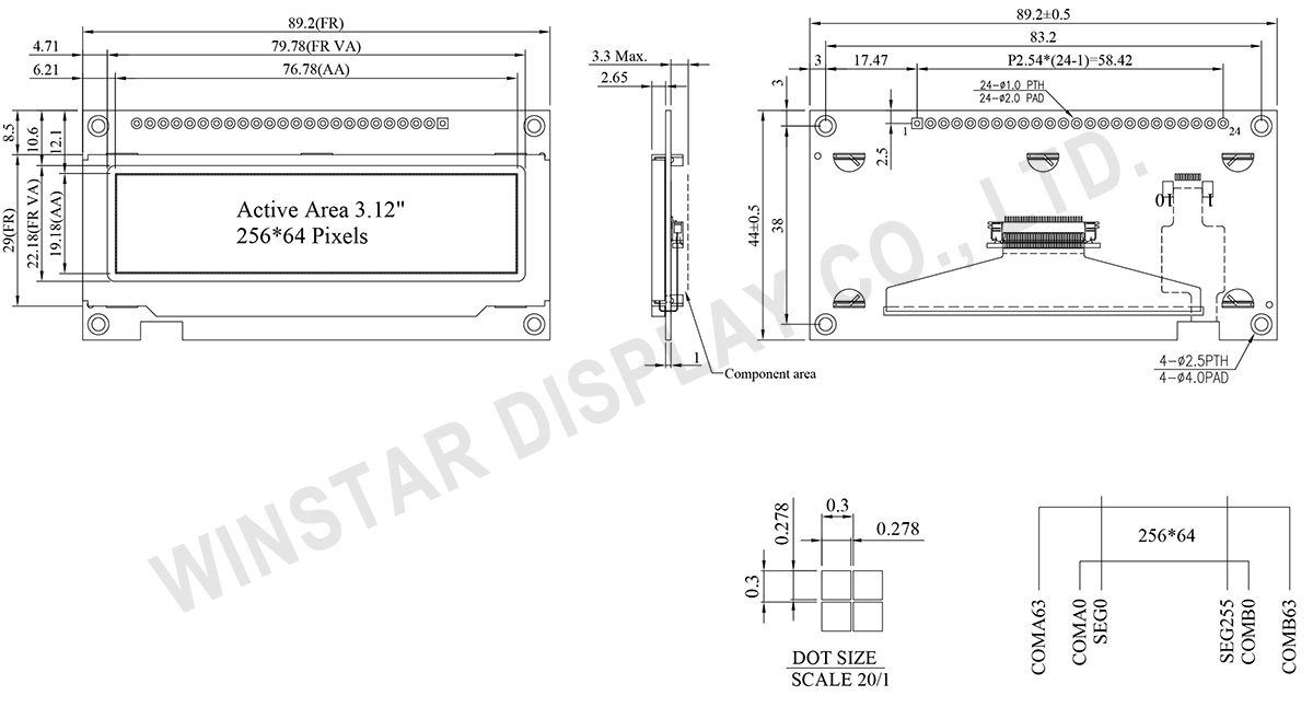
Home Produtos Display OLED Display OLED Gráfico WEN025664B

Model No. WEN025664B

►Tipo: Gráfico
►Estrutura: COF+PCB+Frame
►Tamanho: 3,12 polegadas
►Matriz de pontos 256x64
►Controlador SSD1322 integrado
►Alimentação +3V
►1/64 duty
►Interface: 6800, 8080, SPI
►Display Color: Branco / Amarelo / Céu azul / Verde
►Support Grayscale

Descrição

O modelo WEN025664B é um OLED Gráfico COF, apresentando um tamanho diagonal de 3,12 polegadas e uma resolução de 256x64 pontos. Este módulo OLED é incorporado com o IC SSD1322 e suporta interfaces SPI de 8 bits 6800/8080 e 3/4 linhas. Possui uma dimensão de contorno de 89,2 × 44,0 mm, com uma área ativa de 76,78 × 19,18 mm. Também suporta 4 bits de escala de cinza, com uma voltagem de alimentação lógica de 3V. A corrente de exibição a 50% do tabuleiro de xadrez é de 150mA @3.0V VDD (valor típico), com um ciclo de acionamento de 1/64.

O módulo possui uma PCB integrada, permitindo que os clientes usem conexões por fio sem a necessidade de desenvolvimento adicional de PCB para suas aplicações. Além disso, o circuito VCC integrado na PCB simplifica o uso pelo cliente. Esta placa PCB, equipada com quatro furos de montagem, fornece um método fácil para os clientes fixarem os módulos em suas aplicações. Este módulo OLED é adequado para aplicações em casas inteligentes, dispositivos médicos, controle industrial, etc.

O modelo WEN025664B pode operar em temperaturas que variam de -40°C a +80°C, com temperaturas de armazenamento variando de -40°C a +85°C. O módulo OLED possui uma alta relação de contraste de 10.000:1, resultando em uma qualidade de imagem aprimorada, detalhes mais nítidos e melhor legibilidade, especialmente em ambientes com pouca luz.

Além disso, painéis OLED com as mesmas dimensões oferecem uma variedade de alternativas:
  • Série WEX025664B sem uma estrutura metálica e PCB.
  • Série WEX025664B-CTP sem uma estrutura metálica, PCB e com uma tela sensível ao toque CTP.
  • Série WEN025664B-CTP com uma estrutura metálica, PCB e tela sensível ao toque CTP.

DRAWING

3.12 inch 256x64 COF OLED Display With PCB and Frame - WEN025664B

Data source ref: WEN025664BWAP3N0000

SPECIFICATIONS

Função do pino de interface

Pin
Number
Símbolo I/O Função
1 VSS P Ground.
2 VDD P Power Supply for Core Logic Circuit
Power supply pin for core logic operation. A capacitor is required to connect between this pin and VSS
3 N.C. P Reserved Pin
The N.C. pin between function pins are reserved for compatible and flexible design.
4 D/C# I Data/Command Control
This pin is Data/Command control pin connecting to the MCU.
When the pin is pulled HIGH, the content at D[7:0] will be interpreted as data.
When the pin is pulled LOW, the content at D[7:0] will be interpreted as command.
5 R/W#
(WR#)
I Read/Write Select or Write
This pin is MCU interface input. When interfacing to a 68XX-series microprocessor, this pin will be used as Read/Write (R/W#) selection input. Pull this pin to “High” for read mode and pull it to “Low” for write mode.
When 80XX interface mode is selected, this pin will be the Write (WR#) input. Data write operation is initiated when this pin is pulled low and the CS# is pulled low.
When serial mode is selected, this pin must be connected to VSS.
6 E/RD# I Read/Write Enable or Read
This pin is MCU interface input.
When interfacing to a 68XX-series microprocessor, this pin will be used as the Enable (E) signal. Read/write operation is initiated when this pin is pulled high and the CS# is pulled low.
When connecting to an 80XX-microprocessor, this pin receives the Read (RD#) signal. Data read operation is initiated when this pin is pulled low and CS# is pulled low.
When serial mode is selected, this pin must be connected to VSS.
7~14 DB0 I/O Host Data Input/Output Bus
These pins are 8-bit bi-directional data bus to be connected to the microprocessor’s data bus.
When serial mode is selected, DB1 will be the serial data input SDIN and DB0 will be the serial clock input SCLK.
DB1
DB2
DB3
DB4
DB5
DB6
DB7
15 NC P Reserved Pin
The N.C. pin between function pins are reserved for compatible and flexible design.
16 RES# I This pin is reset signal input.
When the pin is pulled LOW, initialization of the chip is executed.
Keep this pin pull HIGH during normal operation.
17 CS# I Data/Command Control
This pin is the chip select input connecting to the MCU. The chip is enabled for MCU communication only when CS# is pulled LOW.

18
NC P Reserved Pin
The N.C. pin between function pins are reserved for compatible and flexible design.
19 BS1 I Communicating Protocol Select
These pins are MCU interface selection input. See the following table:
BS:[1:0] Bus Interface Selection
00 4 line SPI
01 3 line SPI
10 8-bit 8080 parallel
11 8-bit 6800 parallel
Note
(1) 0 is connected to VSS
(2) 1 is connected to VDD
20 BS0
21~24 NC P Reserved Pin
The N.C. pin between function pins are reserved for compatible and flexible design.

Especificações Gerais

Item Dimensão Unidade
Matriz de pontos 256 x 64 Dots
Dimensão do módulo 89.2 × 44.0 × 3.3 Max. mm
Área ativa 76.78 × 19.18 mm
Tamanho do ponto 0.278 × 0.278 mm
Distância entre pontos 0.3 × 0.3 mm
Modo de exibição Passive Matrix
Cor de exibição Monochrome
Drive Duty 1/64 Duty
Gray Scale 4 bits
IC SSD1322 (COF)
Interface 6800, 8080, SPI
Size 3.12 polegadas

Classificações Máximas Absolutas

Parameter Símbolo Valor Min Valor Máximo Unidade
Supply Voltage for Display VDD -0.3 4 V
Temperatura de operação TOP -40 80 °C
Temperatura de armazenamento TSTG -40 85 °C

Características Eletrônicas

Item Símbolo Condition Valor Min Typ Valor Máximo Unidade
Supply Voltage for Logic VDD 2.8 3.0 3.3 V
High Level Input VIH 0.8×VDD VDD V
Low Level Input VIL 0 0.2×VDD V
High Level Output VOH 0.9×VDD VDD V
Low Level Output VOL 0 0.1×VDD V
50% Check Board operating Current IDD VCC =3V 150 300 mA
 

Search keyword: 256x64 oled, oled 256x64, 3.12 oled, 3.12" oled, 3.12 inch oled, oled 3.12, oled 3.12"

go top
close