 - WLEP02566400DGAAASA00")
 - WEO025664D-CTP")
 - WEO025664E")
私たちはあなたのプライバシーを大切にします
「すべてのクッキーを許可」をクリックすると、サイトのナビゲーションを向上させ、サイト使用状況を分析し、マーケティングおよびパフォーマンスの取り組みを支援するために、クッキーをデバイスに保存することに同意したことになります。この件に関する詳細情報は、ポリシーをご覧ください。プライバシーポリシー

 - WEO025664D")
 - WEO025664D")
 - WEO025664D")
 - WEO025664D")
 - WEO025664D")
WEO025664Dは、解像度256×64ドットの3.55インチCOG構造グラフィックOLEDディスプレイです。SSD1322コントローラICを搭載し、4ビットグレースケール表示に対応しています。インターフェースは6800/8080パラレルおよび3線/4線SPIをサポートします。高コントラストおよび広視野角特性により、さまざまな照明環境下で安定した視認性を確保します。
本モデルはロジック電圧3.3V、表示駆動電圧16Vで動作します。標準消費電流は35mA(VCC=16V、50%チェッカーボードパターン時)です。駆動方式は1/64デューティを採用しています。
本ディスプレイは、医療機器、操作パネル、セルフレジ端末、券売機、パーキングメーターなど、コンパクトなモノクロOLED表示を必要とする機器に適用可能です。動作温度範囲は-40℃~+80℃、保存温度範囲は-40℃~+85℃です。
| 項目 | 仕様 | 単位 |
|---|---|---|
| ドットマトリックス(解像度) | 256 x 64 | - |
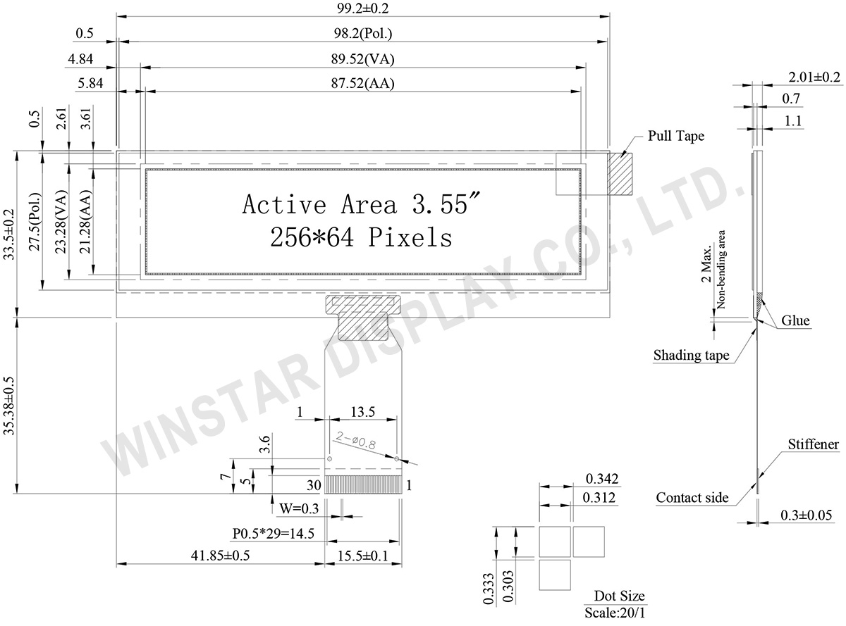
| 外形寸法 | 99.2 × 33.5 × 2.01 | mm |
| 有効表示エリア | 87.52 × 21.28 | mm |
| ドットサイズ | 0.312 × 0.303 | mm |
| ドットピッチ | 0.342 × 0.333 | mm |
| 表示モード | パッシブマトリクス | |
| 発光色 | モノクロ | |
| 駆動方法 | 1/64 Duty | |
| グレースケール | 4 bits | |
| IC | SSD1322 | |
| インターフェイス | 6800, 8080, SPI | |
| サイズ | 3.55 インチ | |
| パラメーター | 記号 | 最小値 | 最大値 | 単位 |
|---|---|---|---|---|
| ロジック電源電圧 | VDD | -0.5 | 2.75 | V |
| 低電圧電源 | VCI | -0.3 | 400 | V |
| I/O pins 電源電圧 | VDDIO | -0.5 | VCI | V |
| Display電源電圧 | VCC | -0.5 | 20 | V |
| 操作温度 | TOP | -40 | 80 | °C |
| 保存温度 | TSTG | -40 | 85 | °C |
| 項目 | 記号 | 条件 | 最小値 | 典型値 | 最大値 | 単位 |
|---|---|---|---|---|---|---|
| 低電源電圧 | VCI | - | 2.4 | 3.3 | 3.5 | V |
| Display電源電圧 | VCC | - | 10.0 | 16.0 | 16.5 | V |
| ロジック電源 | VDD | - | 2.4 | - | 2.6 | V |
| I/O pins 電源 | VDDIO | - | 1.65 | VCI | V | |
| 入力電圧(High) | VIH | - | 0.8×VDDIO | - | VDDIO | V |
| 入力電圧(Low) | VIL | - | 0 | - | 0.2×VDDIO | V |
| 出力電圧(High) | VOH | - | 0.9×VDDIO | - | VDDIO | V |
| 出力電圧(Low) | VOL | - | 0 | - | 0.1×VDDIO | V |
| ディスプレイ50%ピクセル点灯 | VCC =16 V | - | - | 35 | 55 | mA |
| Pin Number | 記号 | I/O | 説明 | ||||||||||
|---|---|---|---|---|---|---|---|---|---|---|---|---|---|
| 1 | ESD_GND | P | Ground | ||||||||||
| 2 | VSS | P | Ground. | ||||||||||
| 3 | VCC | P | Power supply for panel driving voltage. This is also the most positive power voltage supply pin. |
||||||||||
| 4 | VCOMH | P | COM signal deselected voltage level. A capacitor should be connected between this pin and VSS. |
||||||||||
| 5 | VLSS | P | Analog system ground pin. | ||||||||||
| 6~13 | D7~D0 | I/O | Host Data Input/Output Bus These pins are 8-bit bi-directional data bus to be connected to the microprocessor’s data bus. When serial mode is selected, D1 will be the serial data input SDIN and D0 will be the serial clock input SCLK. |
||||||||||
| 14 | E/RD# | I | Read/Write Enable or Read This pin is MCU interface input. When interfacing to a 68XX-series microprocessor, this pin will be used as the Enable (E) signal. Read/write operation is initiated when this pin is pulled high and the CS# is pulled low. When connecting to an 80XX-microprocessor, this pin receives the Read (RD#) signal. Data read operation is initiated when this pin is pulled low and CS# is pulled low. When serial mode is selected, this pin must be connected to VSS. |
||||||||||
| 15 | R/W# | I | Read/Write Select or Write This pin is MCU interface input. When interfacing to a 68XX-series microprocessor, this pin will be used as Read/Write (R/W#) selection input. Pull this pin to “High” for read mode and pull it to “Low” for write mode. When 80XX interface mode is selected, this pin will be the Write (WR#) input. Data write operation is initiated when this pin is pulled low and the CS# is pulled low. When serial mode is selected, this pin must be connected to VSS. |
||||||||||
| 16 | BS0 | I | Communicating Protocol Select These pins are MCU interface selection input. See the following table:
Note (1) 0 is connected to VSS (2) 1 is connected to VDDIO |
||||||||||
| 17 | BS1 | ||||||||||||
| 18 | D/C# | I | Data/Command Control This pin is Data/Command control pin connecting to the MCU. When the pin is pulled HIGH, the content at D[7:0] will be interpreted as data. When the pin is pulled LOW, the content at D[7:0] will be interpreted as command. |
||||||||||
| 19 | CS# | I | Data/Command Control This pin is the chip select input connecting to the MCU. The chip is enabled for MCU communication only when CS# is pulled LOW. |
||||||||||
| 20 | RES# | I | This pin is reset signal input. When the pin is pulled LOW, initialization of the chip is executed. Keep this pin pull HIGH during normal operation. |
||||||||||
| 21 | FR | O | This pin is No Connection pins. Nothing should be connected to this pin. This pin should be left open individually. | ||||||||||
| 22 | IREF | I | Current Reference for Brightness Adjustment This pin is segment current reference pin. A resistor should be connected between this pin and VSS. Set the current lower than 10uA. |
||||||||||
| 23 | N.C. | - | Reserved Pin The N.C. pin between function pins are reserved for compatible and flexible design. |
||||||||||
| 24 | VDDIO | P | Power Supply for I/O Pin It should be matched with the MCU interface voltage level. |
||||||||||
| 25 | VDD | P | Power Supply for Core Logic Circuit Power supply pin for core logic operation. A capacitor is required to connect between this pin and VSS |
||||||||||
| 26 | VCI | P | Power Supply for Operation VCI must always be equal to or higher than VDD and VDDIO. |
||||||||||
| 27 | VSL | P | Voltage Output Low Level for SEG Signal This is segment voltage reference pin. When external VSL is not used, this pin should be left open. When external VSL is used, this pin should connect with resistor and diode to ground. |
||||||||||
| 28 | VLSS | P | Ground of Analog Circuit These are the analog ground pins. They should be connected to VSS externally. |
||||||||||
| 29 | VCC | P | Power Supply for OLED Panel These are the most positive voltage supply pin of the chip. They must be connected to external source. |
||||||||||
| 30 | ESD GND | P | Ground |

「すべてのクッキーを許可」をクリックすると、サイトのナビゲーションを向上させ、サイト使用状況を分析し、マーケティングおよびパフォーマンスの取り組みを支援するために、クッキーをデバイスに保存することに同意したことになります。この件に関する詳細情報は、ポリシーをご覧ください。プライバシーポリシー