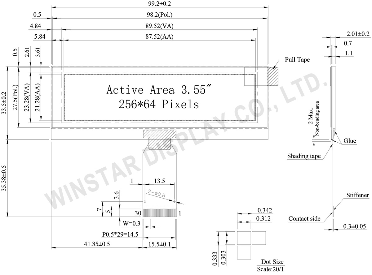
| Pin Number |
Sembol |
I/O |
Fonksiyon |
| 1 |
ESD_GND |
P |
Ground |
| 2 |
VSS |
P |
Ground. |
| 3 |
VCC |
P |
Power supply for panel driving voltage.
This is also the most positive power voltage supply pin. |
| 4 |
VCOMH |
P |
COM signal deselected voltage level.
A capacitor should be connected between this pin and VSS. |
| 5 |
VLSS |
P |
Analog system ground pin. |
| 6~13 |
D7~D0 |
I/O |
Host Data Input/Output Bus
These pins are 8-bit bi-directional data bus to be connected to the microprocessor’s data bus.
When serial mode is selected, D1 will be the serial data input SDIN and D0 will be the serial clock input SCLK. |
| 14 |
E/RD# |
I |
Read/Write Enable or Read
This pin is MCU interface input.
When interfacing to a 68XX-series microprocessor, this pin will be used as the Enable (E) signal. Read/write operation is initiated when this pin is pulled high and the CS# is pulled low.
When connecting to an 80XX-microprocessor, this pin receives the Read (RD#) signal. Data read operation is initiated when this pin is pulled low and CS# is pulled low.
When serial mode is selected, this pin must be connected to VSS. |
| 15 |
R/W# |
I |
Read/Write Select or Write
This pin is MCU interface input. When interfacing to a 68XX-series microprocessor, this pin will be used as Read/Write (R/W#) selection input. Pull this pin to “High” for read mode and pull it to “Low” for write mode.
When 80XX interface mode is selected, this pin will be the Write (WR#) input. Data write operation is initiated when this pin is pulled low and the CS# is pulled low.
When serial mode is selected, this pin must be connected to VSS. |
| 16 |
BS0 |
I |
Communicating Protocol Select
These pins are MCU interface selection input. See the following table:
| BS[1:0] |
Bus Interface Selection |
| 00 |
4 line SPI |
| 01 |
3 line SPI |
| 10 |
8-bit 8080 parallel |
| 11 |
8-bit 6800 parallel |
Note
(1) 0 is connected to VSS
(2) 1 is connected to VDDIO |
| 17 |
BS1 |
| 18 |
D/C# |
I |
Data/Command Control
This pin is Data/Command control pin connecting to the MCU.
When the pin is pulled HIGH, the content at D[7:0] will be interpreted as data.
When the pin is pulled LOW, the content at D[7:0] will be interpreted as command. |
| 19 |
CS# |
I |
Data/Command Control
This pin is the chip select input connecting to the MCU. The chip is enabled for MCU communication only when CS# is pulled LOW. |
| 20 |
RES# |
I |
This pin is reset signal input.
When the pin is pulled LOW, initialization of the chip is executed.
Keep this pin pull HIGH during normal operation. |
| 21 |
FR |
O |
This pin is No Connection pins. Nothing should be connected to this pin. This pin should be left open individually. |
| 22 |
IREF |
I |
Current Reference for Brightness Adjustment
This pin is segment current reference pin. A resistor should be connected between this pin and VSS. Set the current lower than 10uA. |
| 23 |
N.C. |
- |
Reserved Pin
The N.C. pin between function pins are reserved for compatible and flexible design. |
| 24 |
VDDIO |
P |
Power Supply for I/O Pin
It should be matched with the MCU interface voltage level. |
| 25 |
VDD |
P |
Power Supply for Core Logic Circuit
Power supply pin for core logic operation. A capacitor is required to connect between this pin and VSS |
| 26 |
VCI |
P |
Power Supply for Operation
VCI must always be equal to or higher than VDD and VDDIO. |
| 27 |
VSL |
P |
Voltage Output Low Level for SEG Signal
This is segment voltage reference pin.
When external VSL is not used, this pin should be left open.
When external VSL is used, this pin should connect with resistor and diode to ground. |
| 28 |
VLSS |
P |
Ground of Analog Circuit
These are the analog ground pins. They should be connected to VSS externally. |
| 29 |
VCC |
P |
Power Supply for OLED Panel
These are the most positive voltage supply pin of the chip. They must be connected to external source. |
| 30 |
ESD GND |
P |
Ground |

