


우리는 귀하의 프라이버시를 소중히 여깁니다
"모든 쿠키 허용"을 클릭하면 사이트 탐색을 개선하고, 사이트 사용을 분석하며, 마케팅 및 성능 노력에 도움을 주기 위해 쿠키를 귀하의 장치에 저장하는 데 동의한 것으로 간주됩니다. 이 주제에 대한 추가 정보는 당사의 정책에서 확인할 수 있습니다. 개인정보 보호정책


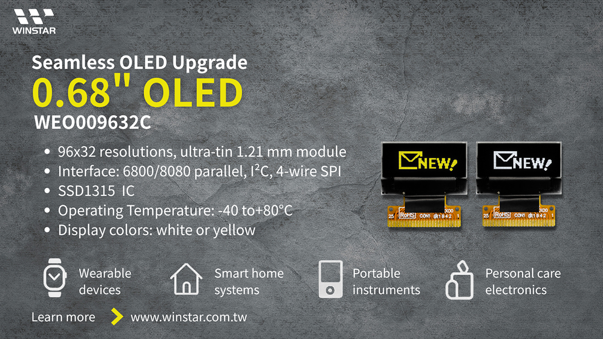
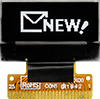
WEO009632C는 96×32 픽셀 해상도와 0.68인치 대각선 크기를 가진 미니 OLED 디스플레이입니다. SSD1315 컨트롤러를 내장하고 있으며, 6800/8080 8비트 병렬, I²C 및 4선식 SPI 인터페이스를 지원합니다. 로직 전원 공급 전압은 3V이며, 1/32 듀티 사이클로 동작하며, 50% 체커보드 패턴에서의 전형적인 디스플레이 전류는 3.6mA @ 12Vcc입니다. 이 OLED 모듈은 -40℃에서 +80℃까지 동작 가능하며, -40℃에서 +85℃까지 보관할 수 있습니다. Winstar는 고객이 응용 분야에 가장 적합한 옵션을 선택할 수 있도록 ZIF FPC와 Hotbar 버전을 모두 제공합니다.
WEO009632C 미니 COG PMOLED 모듈은 두께가 단지 1.21mm로 초슬림하고, 가볍고, 저전력 소비가 특징입니다. 웨어러블 기기, 스마트 홈 응용 제품, 휴대용 기기, 계측기, 개인 관리 기기, 음성 녹음 펜, 헬스케어 기기 등 다양한 분야에 이상적입니다.
 FPC 옵션
| 항목 | 치수 | 단위 |
|---|---|---|
| 해상도 | 96 × 32 | 점 |
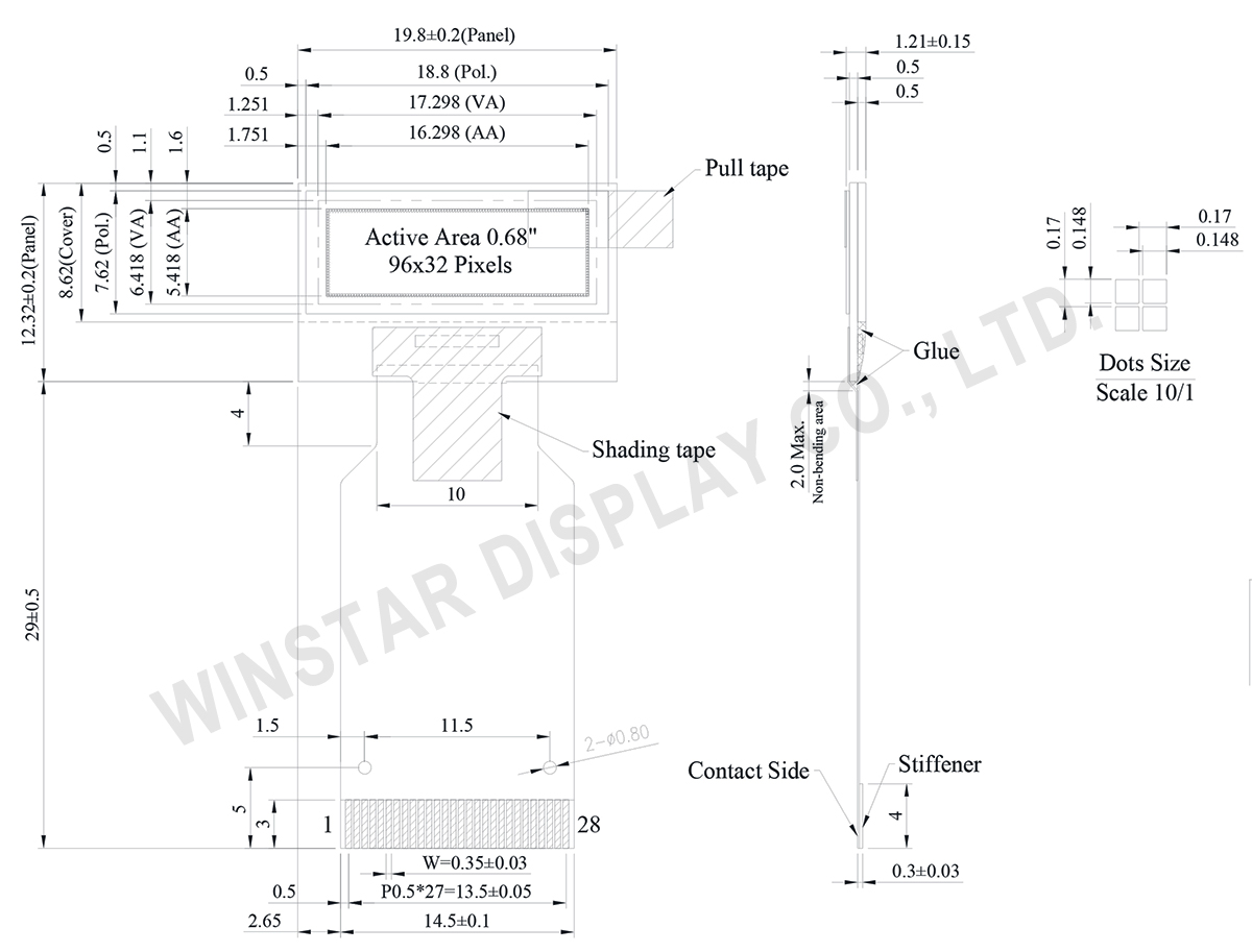
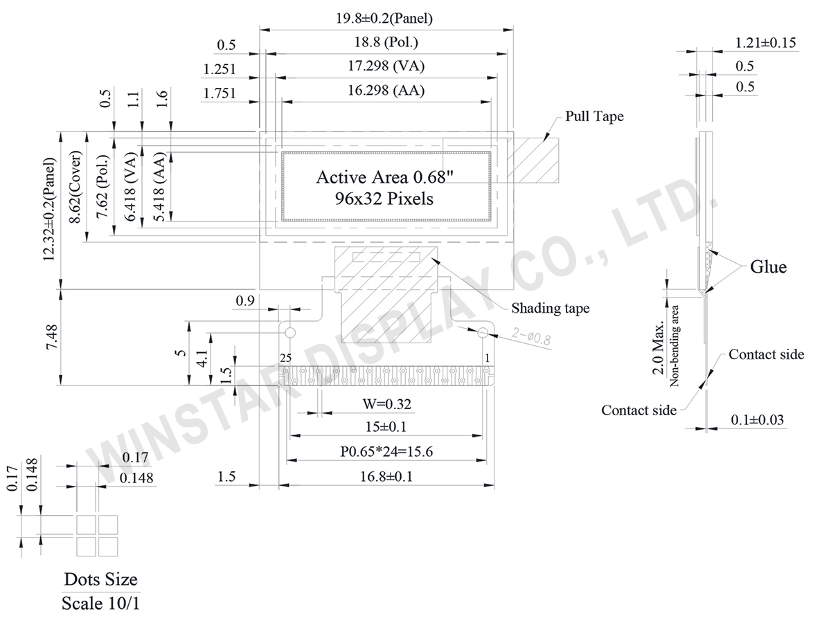
| 모듈 치수 | 19.80 × 12.32 × 1.21 | mm |
| 활성 영역 | 16.298 × 5.418 | mm |
| 도트 크기 | 0.148 × 0.148 | mm |
| 도트 피치 | 0.17 × 0.17 | mm |
| 디스플레이 모드 | 패시브 매트릭스 | |
| 디스플레이 색상 | 단색 | |
| 구동 듀티 | 1/32 Duty | |
| IC | SSD1315 | |
| 인터페이스 | 6800, 8080,4-Wire SPI, I2C | |
| 크기 | 0.68 인치 | |
| 매개변수 | 기호 | 최소값 | 대표값 | 최대값 | 단위 |
|---|---|---|---|---|---|
| Supply Voltage for Logic | VDD | -0.3 | - | 4 | V |
| Supply Voltage for Display | VCC | 0 | - | 18 | V |
| 작동 온도 | TOP | -40 | - | +80 | °C |
| 보관 온도 | TSTG | -40 | - | +85 | °C |
| 항목 | 기호 | 조건 | 최소값 | 대표값 | 최대값 | 단위 |
|---|---|---|---|---|---|---|
| Supply Voltage for Logic | VDD | - | 1.65 | 3.0 | 3.3 | V |
| Supply Voltage for Display | VCC | - | 7.5 | 12.0 | 12.5 | V |
| High Level Input | VIH | - | 0.8×VDD | - | VDD | V |
| Low Level Input | VIL | - | 0 | - | 0.2×VDD | V |
| High Level Output | VOH | Iout = 100uA | 0.9×VDD | - | VDD | V |
| Low Level Output | VOL | Iout = 100uA | 0 | - | 0.1×VDD | V |
| Display 50% Pixel on | ICC | VCC=12V | - | 5.0 | 7.5 | mA |
| No. | 기호 | 기능 | ||||||||||
|---|---|---|---|---|---|---|---|---|---|---|---|---|
| 1 | VSS | Ground pin. It must be connected to external ground. | ||||||||||
| 2 | NC | No connection | ||||||||||
| 3 | VDD | Power supply pin for core logic operation. | ||||||||||
| 4~8 | NC | No connection | ||||||||||
| 9 | VDD | Power supply pin for core logic operation. | ||||||||||
| 10 | BS1 | MCU bus interface selection pins. Select appropriate logic setting as described in the following table. BS2, BS1 are pin select
(1) 0 is connected to VSS (2) 1 is connected to VDD |
||||||||||
| 11 | BS2 | |||||||||||
| 12 | NC | No connection | ||||||||||
| 13 | CS# | This pin is the chip select input connecting to the MCU. The chip is enabled for MCU communication only when CS# is pulled LOW (active LOW). |
||||||||||
| 14 | RES# | This pin is reset signal input. When the pin is pulled LOW, initialization of the chip is executed. Keep this pin HIGH (i.e. connect to VDD) during normal operation. | ||||||||||
| 15 | D/C# | This pin is Data/Command control pin connecting to the MCU. When the pin is pulled HIGH, the data at D[7:0] will be interpreted as data. When the pin is pulled LOW, the data at D[7:0] will be transferred to a command register. In I2C mode, this pin acts as SA0 for slave address selection. |
||||||||||
| 16 | W/R# | This is read / write control input pin connecting to the MCU interface. When interfacing to a 6800-series microprocessor, this pin will be used as Read/Write (R/W#) selection input. Read mode will be carried out when this pin is pulled HIGH (i.e. connect to VDD) and write mode when LOW. When 8080 interface mode is selected, this pin will be the Write (WR#) input. Data write operation is initiated when this pin is pulled LOW and the chip is selected. When serial or I2C interface is selected, this pin must be connected to VSS. |
||||||||||
| 17 | E/RD# | This pin is MCU interface input. When 6800 interface mode is selected, this pin will be used as the Enable (E) signal. Read/write operation is initiated when this pin is pulled HIGH and the chip is selected. When 8080 interface mode is selected, this pin receives the Read (RD#) signal. Read operation is initiated when this pin is pulled LOW and the chip is selected. When serial or I2C interface is selected, this pin must be connected to VSS. |
||||||||||
| 18 | D0 | These are 8-bit bi-directional data bus to be connected to the microprocessor’s data bus. When serial interface mode is selected, D0 will be the serial clock input: SCLK; D1 will be the serial data input: SDIN. When I2C mode is selected, D2, D1 should be tied together and serve as SDAout, SDAin in application and D0 is the serial clock input, SCL. |
||||||||||
| 19 | D1 | |||||||||||
| 20 | D2 | |||||||||||
| 21 | D3 | |||||||||||
| 22 | D4 | |||||||||||
| 23 | D5 | |||||||||||
| 24 | D6 | |||||||||||
| 25 | D7 | |||||||||||
| 26 | IREF | This is segment output current reference pin. When external IREF is used, a resistor should be connected between this pin and VSS to maintain the IREF current at 30uA. |
||||||||||
| 27 | VCOMH | COM signal deselected voltage level. A capacitor should be connected between this pin and VSS. |
||||||||||
| 28 | VCC | Power supply for panel driving voltage. This is also the most positive power voltage supply pin. |
| 그림 | FPC Length | PIN | pitch | ZIF FPC or HOTBAR FPC | 인터페이스 | FPC No. | Create Date |
|---|---|---|---|---|---|---|---|
 |
30 | 28 | 0.5 | ZIF FPC | 6800, 8080,4-Wire SPI, I2C | FPC2050002811XXXXX01 | 20180131 |
 |
8.479 | 25 | 0.65 | HOTBAR FPC | 6800, 8080,4-Wire SPI, I2C | FPC2065002501XXXXX00 | 20190906 |

"모든 쿠키 허용"을 클릭하면 사이트 탐색을 개선하고, 사이트 사용을 분석하며, 마케팅 및 성능 노력에 도움을 주기 위해 쿠키를 귀하의 장치에 저장하는 데 동의한 것으로 간주됩니다. 이 주제에 대한 추가 정보는 당사의 정책에서 확인할 수 있습니다. 개인정보 보호정책