
 - WEX025664B-CTP")

")
私たちはあなたのプライバシーを大切にします
「すべてのクッキーを許可」をクリックすると、サイトのナビゲーションを向上させ、サイト使用状況を分析し、マーケティングおよびパフォーマンスの取り組みを支援するために、クッキーをデバイスに保存することに同意したことになります。この件に関する詳細情報は、ポリシーをご覧ください。プライバシーポリシー


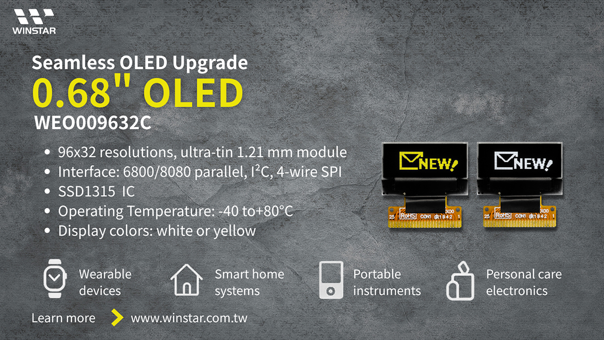
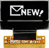
WEO009632Cは0.68インチ・96x32ドット・ミニOLEDディスプレーです。SSD1315 ICを内蔵し、6800/8080 8-ビットパラレル、I2Cと4線式SPIインターフェースをサポートできます。供給電圧は3V、Duty数は1/32です。チェックボード(市松模様、表示エリアが50%程度点灯する)を表示させる場合、消耗電流値は3.6mA@12Vcc (典型値)となり、操作温度は-40℃~+80℃で、保存温度は-40℃~+85℃です。お客様がアプリケーションに適したモジュールを選択できるように、ZIF FPC及びHotbarバージョンを提供しています。
COG PMOLEDモジュールですので、バックライトは要りません。その故、この製品の厚さはただ1.21mmです。軽くて低消費電流のこの製品はウェアラブルデバイス、スマートホームアプリケーション、ポータブルデバイス、メーターデバイス、パーソナルケア機器、ボイスレコーダーペン、ヘルスデバイスなどに適しています。
 FPC Options
| 項目 | 仕様 | 単位 |
|---|---|---|
| 解像度 | 96 × 32 | Dots |
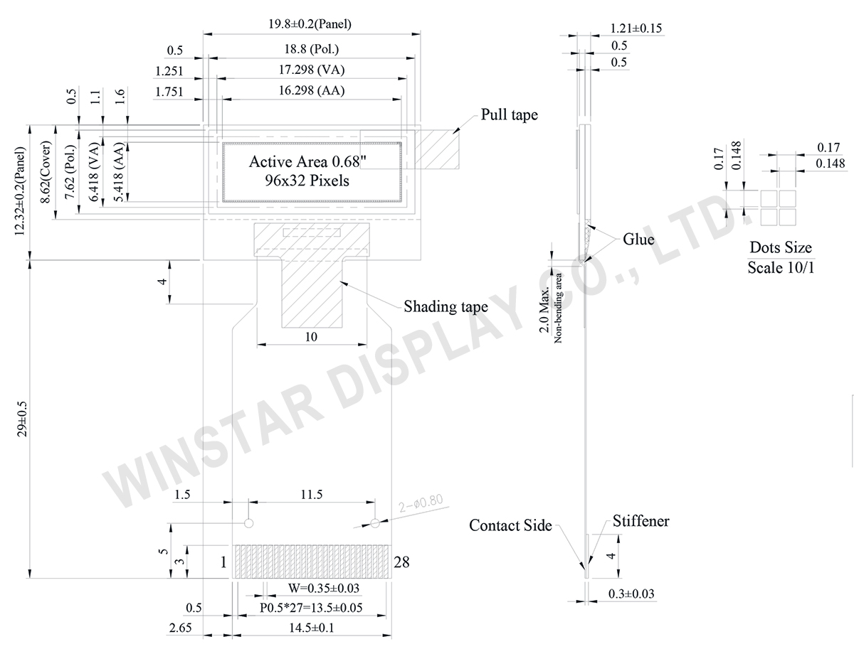
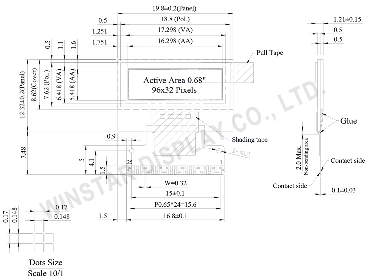
| 外形寸法 | 19.80 × 12.32 × 1.21 | mm |
| 有効エリア | 16.298 × 5.418 | mm |
| ピクセルサイズ | 0.148 × 0.148 | mm |
| ピクセルピッチ | 0.17 × 0.17 | mm |
| 表示モード | パッシブマトリクス | |
| 発光色 | モノクロ | |
| 駆動方法 | 1/32 Duty | |
| IC | SSD1315 | |
| インターフェイス | 6800, 8080,4-Wire SPI, I2C | |
| サイズ | 0.68 インチ | |
| パラメーター | 記号 | 最小値 | 典型値 | 最大値 | 単位 |
|---|---|---|---|---|---|
| ロジック電源電圧 | VDD | -0.3 | - | 4 | V |
| Display電源電圧 | VCC | 0 | - | 18 | V |
| 操作温度 | TOP | -40 | - | +80 | °C |
| 保存温度 | TSTG | -40 | - | +85 | °C |
| 項目 | 記号 | 条件 | 最小値 | 典型値 | 最大値 | 単位 |
|---|---|---|---|---|---|---|
| ロジック電源電圧 | VDD | - | 1.65 | 3.0 | 3.3 | V |
| Display電源電圧 | VCC | - | 7.5 | 12.0 | 12.5 | V |
| 高レベル入力 | VIH | - | 0.8×VDD | - | VDD | V |
| 低レベル入力 | VIL | - | 0 | - | 0.2×VDD | V |
| 高レベル出力 | VOH | Iout = 100uA | 0.9×VDD | - | VDD | V |
| 低レベル出力 | VOL | Iout = 100uA | 0 | - | 0.1×VDD | V |
| Display 50% Pixel on | ICC | VCC=12V | - | 5.0 | 7.5 | mA |
| No. | 記号 | 功能 | ||||||||||
|---|---|---|---|---|---|---|---|---|---|---|---|---|
| 1 | VSS | Ground pin. It must be connected to external ground. | ||||||||||
| 2 | NC | No connection | ||||||||||
| 3 | VDD | Power supply pin for core logic operation. | ||||||||||
| 4~8 | NC | No connection | ||||||||||
| 9 | VDD | Power supply pin for core logic operation. | ||||||||||
| 10 | BS1 | MCU bus interface selection pins. Select appropriate logic setting as described in the following table. BS2, BS1 are pin select
(1) 0 is connected to VSS (2) 1 is connected to VDD |
||||||||||
| 11 | BS2 | |||||||||||
| 12 | NC | No connection | ||||||||||
| 13 | CS# | This pin is the chip select input connecting to the MCU. The chip is enabled for MCU communication only when CS# is pulled LOW (active LOW). |
||||||||||
| 14 | RES# | This pin is reset signal input. When the pin is pulled LOW, initialization of the chip is executed. Keep this pin HIGH (i.e. connect to VDD) during normal operation. | ||||||||||
| 15 | D/C# | This pin is Data/Command control pin connecting to the MCU. When the pin is pulled HIGH, the data at D[7:0] will be interpreted as data. When the pin is pulled LOW, the data at D[7:0] will be transferred to a command register. In I2C mode, this pin acts as SA0 for slave address selection. |
||||||||||
| 16 | W/R# | This is read / write control input pin connecting to the MCU interface. When interfacing to a 6800-series microprocessor, this pin will be used as Read/Write (R/W#) selection input. Read mode will be carried out when this pin is pulled HIGH (i.e. connect to VDD) and write mode when LOW. When 8080 interface mode is selected, this pin will be the Write (WR#) input. Data write operation is initiated when this pin is pulled LOW and the chip is selected. When serial or I2C interface is selected, this pin must be connected to VSS. |
||||||||||
| 17 | E/RD# | This pin is MCU interface input. When 6800 interface mode is selected, this pin will be used as the Enable (E) signal. Read/write operation is initiated when this pin is pulled HIGH and the chip is selected. When 8080 interface mode is selected, this pin receives the Read (RD#) signal. Read operation is initiated when this pin is pulled LOW and the chip is selected. When serial or I2C interface is selected, this pin must be connected to VSS. |
||||||||||
| 18 | D0 | These are 8-bit bi-directional data bus to be connected to the microprocessor’s data bus. When serial interface mode is selected, D0 will be the serial clock input: SCLK; D1 will be the serial data input: SDIN. When I2C mode is selected, D2, D1 should be tied together and serve as SDAout, SDAin in application and D0 is the serial clock input, SCL. |
||||||||||
| 19 | D1 | |||||||||||
| 20 | D2 | |||||||||||
| 21 | D3 | |||||||||||
| 22 | D4 | |||||||||||
| 23 | D5 | |||||||||||
| 24 | D6 | |||||||||||
| 25 | D7 | |||||||||||
| 26 | IREF | This is segment output current reference pin. When external IREF is used, a resistor should be connected between this pin and VSS to maintain the IREF current at 30uA. |
||||||||||
| 27 | VCOMH | COM signal deselected voltage level. A capacitor should be connected between this pin and VSS. |
||||||||||
| 28 | VCC | Power supply for panel driving voltage. This is also the most positive power voltage supply pin. |
| Drawing | FPC Length | PIN | pitch | ZIF FPC or HOTBAR FPC | Interface | FPC No. | Create Date |
|---|---|---|---|---|---|---|---|
 |
30 | 28 | 0.5 | ZIF FPC | 6800, 8080,4-Wire SPI, I2C | FPC2050002811XXXXX01 | 20180131 |
 |
8.479 | 25 | 0.65 | HOTBAR FPC | 6800, 8080,4-Wire SPI, I2C | FPC2065002501XXXXX00 | 20190906 |

「すべてのクッキーを許可」をクリックすると、サイトのナビゲーションを向上させ、サイト使用状況を分析し、マーケティングおよびパフォーマンスの取り組みを支援するために、クッキーをデバイスに保存することに同意したことになります。この件に関する詳細情報は、ポリシーをご覧ください。プライバシーポリシー