
私たちはあなたのプライバシーを大切にします
「すべてのクッキーを許可」をクリックすると、サイトのナビゲーションを向上させ、サイト使用状況を分析し、マーケティングおよびパフォーマンスの取り組みを支援するために、クッキーをデバイスに保存することに同意したことになります。この件に関する詳細情報は、ポリシーをご覧ください。プライバシーポリシー

- WEO006448B")
- WEO006448B")
- WEO006448B")
- WEO006448B")
- WEO006448B")
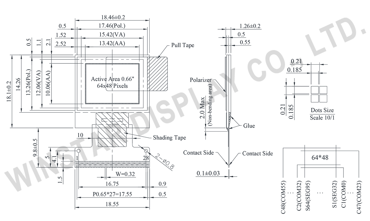
WEO006448Bモデルは、0.66インチの対角サイズと64x48ドットの解像度を持つ消費者向けCOG OLEDディスプレイです。このOLEDモジュールは、SSD1315 ICと統合されており、6800、8080、4ワイヤSPI、およびI2Cインターフェースをサポートしています。論理回路の供給電圧は3V、表示の供給電圧は7.5Vです。ディスプレイの通常の消費電流は、50%の明暗パターン時で、7.5V VCCにて3mA、駆動デューティは1/48です。このモジュールは、内部電圧変換回路(チャージポンプ)と外部VCC供給の両方に対応しています。
このモデルは、Bluetoothスピーカーやアンプ、USBデバイス、ポータブルガジェット、健康管理デバイス、デジタルメーター、および計測機器などの消費者向けアプリケーションに適しています。動作温度範囲は-30℃から+70℃、保存温度範囲は-30℃から+70℃です。
| 項目 | 仕様 | 単位 |
|---|---|---|
| ドットマトリックス(解像度) | 64 x 48 Dots | - |
| モジュールサイズ | 18.46 × 18.10 × 1.26 | mm |
| 有効エリア | 13.42 × 10.06 | mm |
| ドットサイズ | 0.185 × 0.185 | mm |
| ドットピッチ | 0.210 × 0.210 | mm |
| 表示モード | パッシブマトリクス | |
| 発光色 | モノクロ | |
| 駆動方法 | 1/48 Duty | |
| IC | SSD1315 | |
| インターフェイス | 6800, 8080, 4-Wire SPI, I2C | |
| 表示サイズ(対角線) | 0.66 インチ | |
| パラメーター | 記号 | 最小值 | 最大值 | 単位 |
|---|---|---|---|---|
| 電源電圧 | VDD | 0 | 4.0 | V |
| チャージポンプレギュレータ供給電圧 | VBAT | 0 | 6.0 | V |
| Display電源電圧 | VCC | 0 | 18.0 | V |
| 操作温度 | TOP | -30 | +70 | °C |
| 保存温度 | TSTG | -30 | +70 | °C |
| 項目 | 記号 | 条件 | 最小值 | 典型值 | 最大值 | 単位 |
|---|---|---|---|---|---|---|
| ロジック電源電圧 | VDD | - | 1.65 | 3.0 | 3.3 | V |
| 表示用電源電圧(外部供給) | VCC | - | 6.0 | 7.5 | 15.0 | V |
| チャージポンプレギュレータ供給電圧 | VBAT | - | 3.0 | 3.3 | VDD | V |
| 用於顯示的電荷泵輸出電壓(由內部 DC/DC 生成) | - | 7.0 | 7.5 | 0.2×VDD | V | |
| 入力電圧(High) | VIH | - | 0.8×VDD | - | VDD | V |
| 入力電圧(Low) | VIL | - | 0 | - | 0.1×VDD | V |
| 出力電圧(High) | VOH | - | 0.9×VDD | - | 30 | V |
| 出力電圧(Low) | VOL | - | 0 | - | 30 | V |
| ディスプレイ 50% ピクセルオン (外部から供給される VCC) | ICC | VCC=7.5V | - | 3 | 30 | mA |
| ディスプレイ 50% ピクセルオン (内部 DC/DC によって生成される VCC) | IBAT | - | - | 15 | 30 | mA |
| No. | 記号 | 説明 | |||||||||||||||
|---|---|---|---|---|---|---|---|---|---|---|---|---|---|---|---|---|---|
| 1 | ESD_GND | It should be connected to ground. | |||||||||||||||
| 2 | C2N | C1P/C1N – Pin for charge pump capacitor; Connect to each other with a capacitor. C2P/C2N – Pin for charge pump capacitor; Connect to each other with a capacitor. |
|||||||||||||||
| 3 | C2P | ||||||||||||||||
| 4 | C1P | ||||||||||||||||
| 5 | C1N | ||||||||||||||||
| 6 | VBAT | Power supply for charge pump regulator circuit.
|
|||||||||||||||
| 7 | VSS | This is a ground pin. | |||||||||||||||
| 8 | VDD | Power supply pin for core logic operation. | |||||||||||||||
| 9 | BS1 | These pins are MCU interface selection input. See the following table.
|
|||||||||||||||
| 10 | BS2 | ||||||||||||||||
| 11 | CS# | The chip is enabled for MCU communication only when CS# is pulled LOW (active LOW). | |||||||||||||||
| 12 | RES# | This pin is reset signal input. When the pin is low, initialization of the chip is executed. Keep this pin HIGH (i.e. connect to VDD) during normal operation. | |||||||||||||||
| 13 | D/C# | This pin is Data/Command control pin connecting to the MCU. When the pin is pulled HIGH, the data at D[7:0] will be interpreted as data. When the pin is pulled LOW, the data at D[7:0] will be transferred. |
|||||||||||||||
| 14 | R/W# | This is read / write control input pin connecting to the MCU interface. When interfacing to a 6800-series microprocessor, this pin will be used as Read/Write (R/W#) selection input. Read mode will be carried out when this pin is pulled HIGH (i.e. connect to VDD) and write mode when LOW. When 8080 interface mode is selected, this pin will be the Write (WR#) input. Data write operation is initiated when this pin is pulled LOW and the chip is selected. When serial or I2C interface is selected, this pin must be connected to VSS. |
|||||||||||||||
| 15 | E/RD# | This pin is MCU interface input. When 6800 interface mode is selected, this pin will be used as the Enable (E) signal. Read/write operation is initiated when this pin is pulled HIGH and the chip is selected. When 8080 interface mode is selected, this pin receives the Read (RD#) signal. Read operation is initiated when this pin is pulled LOW and the chip is selected. When serial or I2C interface is selected, this pin must be connected to VSS |
|||||||||||||||
| 16~23 | D0~D7 | These are 8-bit bi-directional data bus to be connected to the microprocessor’s data bus. When serial interface mode is selected, D0 will be the serial clock input: SCLK; D1 will be the serial data input: SDIN. When I2C mode is selected, D2, D1 should be tied together and serve as SDAout, SDAin in application and D0 is the serial clock input, SCL . | |||||||||||||||
| 24 | IREF | This is segment output current reference pin. When external IREF is used, a resistor should be connected between this pin and VSS to maintain the IREF current at 30uA. When internal IREF is used, this pin should be kept NC. |
|||||||||||||||
| 25 | VCOMH | COM signal deselected voltage level. A capacitor should be connected between this pin and VSS. |
|||||||||||||||
| 26 | VCC | Power supply for panel driving voltage. This is also the most positive power voltage supply pin When charge pump is enabled, a capacitor should be connected between this pin and VSS. |
|||||||||||||||
| 27 | VLSS | This is an analog ground pin. It should be connected to VSS externally. | |||||||||||||||
| 28 | ESD GND | It should be connected to ground. |

「すべてのクッキーを許可」をクリックすると、サイトのナビゲーションを向上させ、サイト使用状況を分析し、マーケティングおよびパフォーマンスの取り組みを支援するために、クッキーをデバイスに保存することに同意したことになります。この件に関する詳細情報は、ポリシーをご覧ください。プライバシーポリシー