我們重視您的隱私
通過點擊「允許所有 Cookie」,代表您同意在您的設備上存儲 Cookie 以增強網站瀏覽體驗、分析網站使用情況並協助我們的行銷和網站效能優化工作。您可以在我們的隱私權政策中找到有關於此的更多資訊。

 - WEO006448B")
 - WEO006448B")
 - WEO006448B")
 - WEO006448B")
 - WEO006448B")
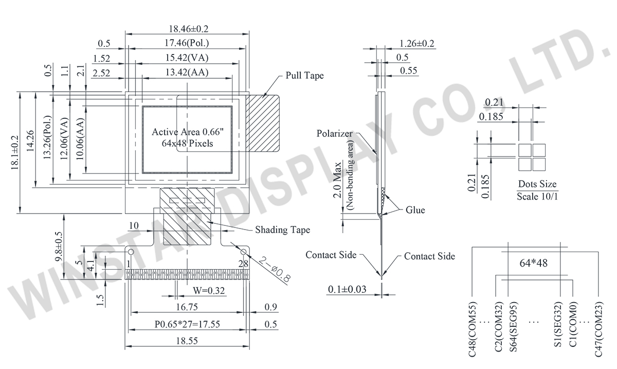
WEO006448B 是一款消費型 0.66 吋 COG OLED 顯示模組,擁有 64x48 點的解析度。此 OLED 模組搭載 SSD1315 IC,支援多種介面,包括 6800、8080、4 線 SPI 以及 I2C。邏輯電壓為 3V,顯示電壓為 7.5V。在顯示為 50% 亮度的情況下,顯示的典型電流為 3mA(在 7.5V VCC 下),驅動方式為 1/48。此模組支援內部電壓轉換器和外部 VCC 供電方式,提供靈活的電源選項。
這款顯示模組適用於各類消費型電子產品,像是藍牙音響與擴大機、USB 裝置、便攜式小工具、健康監控裝置、數位儀表以及各類測量儀器。其工作溫度範圍為 -30℃ 到 +70℃,儲存溫度範圍則為 -30℃ 到 +70℃,能夠滿足多種應用需求。
| 項目 | 尺寸 | 單位 |
|---|---|---|
| 點陣(解析度) | 64 x 48 Dots | - |
| 模組尺寸 | 18.46 × 18.10 × 1.26 | mm |
| 有效區域 | 13.42 × 10.06 | mm |
| 像素大小 | 0.185 × 0.185 | mm |
| 像素間距 | 0.210 × 0.210 | mm |
| 顯示模式 | 被動矩陣 | |
| 顯示顏色 | 單色 | |
| 驅動方式 | 1/48 Duty | |
| IC | SSD1315 | |
| 介面 | 6800, 8080, 4線SPI, I2C | |
| 尺寸 | 0.66 吋 | |
| 參數 | 符號 | 最小值 | 最大值 | 單位 |
|---|---|---|---|---|
| 電源電壓 | VDD | 0 | 4.0 | V |
| 電荷幫浦穩壓器電源電壓 | VBAT | 0 | 6.0 | V |
| 顯示電源電壓 | VCC | 0 | 18.0 | V |
| 工作溫度 | TOP | -30 | +70 | °C |
| 儲存溫度 | TSTG | -30 | +70 | °C |
| 項目 | 符號 | 條件 | 最小值 | 典型值 | 最大值 | 單位 |
|---|---|---|---|---|---|---|
| 邏輯電源電壓 | VDD | - | 1.65 | 3.0 | 3.3 | V |
| 顯示電源電壓(外部提供) | VCC | - | 6.0 | 7.5 | 15.0 | V |
| 電荷幫浦穩壓器電源電壓 | VBAT | - | 3.0 | 3.3 | VDD | V |
| 用於顯示的電荷泵輸出電壓(由內部 DC/DC 生成) | - | 7.0 | 7.5 | 0.2×VDD | V | |
| 輸入高電壓 | VIH | - | 0.8×VDD | - | VDD | V |
| 輸入低電壓 | VIL | - | 0 | - | 0.1×VDD | V |
| 輸出高電壓 | VOH | - | 0.9×VDD | - | 30 | V |
| 輸出低電壓 | VOL | - | 0 | - | 30 | V |
| 顯示 50% 像素(外部提供 VCC) | ICC | VCC=7.5V | - | 3 | 30 | mA |
| 在(由內部 DC/DC 生成的 VCC)上顯示 50% 像素 | IBAT | - | - | 15 | 30 | mA |
| No. | 符號 | 功能說明 | |||||||||||||||
|---|---|---|---|---|---|---|---|---|---|---|---|---|---|---|---|---|---|
| 1 | ESD_GND | It should be connected to ground. | |||||||||||||||
| 2 | C2N | C1P/C1N – Pin for charge pump capacitor; Connect to each other with a capacitor. C2P/C2N – Pin for charge pump capacitor; Connect to each other with a capacitor. |
|||||||||||||||
| 3 | C2P | ||||||||||||||||
| 4 | C1P | ||||||||||||||||
| 5 | C1N | ||||||||||||||||
| 6 | VBAT | Power supply for charge pump regulator circuit.
|
|||||||||||||||
| 7 | VSS | This is a ground pin. | |||||||||||||||
| 8 | VDD | Power supply pin for core logic operation. | |||||||||||||||
| 9 | BS1 | These pins are MCU interface selection input. See the following table.
|
|||||||||||||||
| 10 | BS2 | ||||||||||||||||
| 11 | CS# | The chip is enabled for MCU communication only when CS# is pulled LOW (active LOW). | |||||||||||||||
| 12 | RES# | This pin is reset signal input. When the pin is low, initialization of the chip is executed. Keep this pin HIGH (i.e. connect to VDD) during normal operation. | |||||||||||||||
| 13 | D/C# | This pin is Data/Command control pin connecting to the MCU. When the pin is pulled HIGH, the data at D[7:0] will be interpreted as data. When the pin is pulled LOW, the data at D[7:0] will be transferred. |
|||||||||||||||
| 14 | R/W# | This is read / write control input pin connecting to the MCU interface. When interfacing to a 6800-series microprocessor, this pin will be used as Read/Write (R/W#) selection input. Read mode will be carried out when this pin is pulled HIGH (i.e. connect to VDD) and write mode when LOW. When 8080 interface mode is selected, this pin will be the Write (WR#) input. Data write operation is initiated when this pin is pulled LOW and the chip is selected. When serial or I2C interface is selected, this pin must be connected to VSS. |
|||||||||||||||
| 15 | E/RD# | This pin is MCU interface input. When 6800 interface mode is selected, this pin will be used as the Enable (E) signal. Read/write operation is initiated when this pin is pulled HIGH and the chip is selected. When 8080 interface mode is selected, this pin receives the Read (RD#) signal. Read operation is initiated when this pin is pulled LOW and the chip is selected. When serial or I2C interface is selected, this pin must be connected to VSS |
|||||||||||||||
| 16~23 | D0~D7 | These are 8-bit bi-directional data bus to be connected to the microprocessor’s data bus. When serial interface mode is selected, D0 will be the serial clock input: SCLK; D1 will be the serial data input: SDIN. When I2C mode is selected, D2, D1 should be tied together and serve as SDAout, SDAin in application and D0 is the serial clock input, SCL . | |||||||||||||||
| 24 | IREF | This is segment output current reference pin. When external IREF is used, a resistor should be connected between this pin and VSS to maintain the IREF current at 30uA. When internal IREF is used, this pin should be kept NC. |
|||||||||||||||
| 25 | VCOMH | COM signal deselected voltage level. A capacitor should be connected between this pin and VSS. |
|||||||||||||||
| 26 | VCC | Power supply for panel driving voltage. This is also the most positive power voltage supply pin When charge pump is enabled, a capacitor should be connected between this pin and VSS. |
|||||||||||||||
| 27 | VLSS | This is an analog ground pin. It should be connected to VSS externally. | |||||||||||||||
| 28 | ESD GND | It should be connected to ground. |

通過點擊「允許所有 Cookie」,代表您同意在您的設備上存儲 Cookie 以增強網站瀏覽體驗、分析網站使用情況並協助我們的行銷和網站效能優化工作。您可以在我們的隱私權政策中找到有關於此的更多資訊。