
私たちはあなたのプライバシーを大切にします
「すべてのクッキーを許可」をクリックすると、サイトのナビゲーションを向上させ、サイト使用状況を分析し、マーケティングおよびパフォーマンスの取り組みを支援するために、クッキーをデバイスに保存することに同意したことになります。この件に関する詳細情報は、ポリシーをご覧ください。プライバシーポリシー


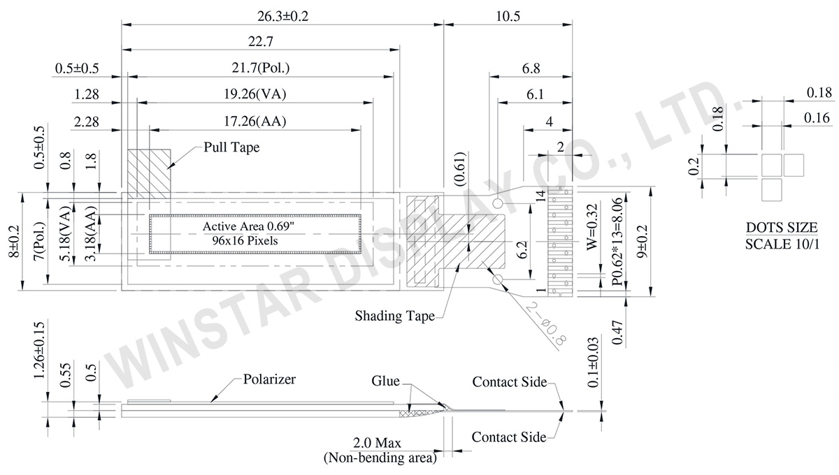
WEO009616Bモデルは消費者向けのCOG小型OLEDディスプレイで、対角サイズは0.69インチで、解像度は96x16ピクセルです。 このOLEDモジュールがSSD1306ICに組み込まれて、 I2Cインターフェースにして、ロジック3V(VDD)の供給電圧で、ディスプレイ7.5V(VCC)の供給電圧で、50%チェックボード電流のディスプレイは5mA @ 7.5V VCC(標準値)で、駆動デューティ1/16をサポートします。内部チャージポンプ電源と外部 VCC 電源をサポートしております。
このWEO009616Bモデルは超薄型、軽量、低消費電力の小型COG有機ELディスプレイです。スマートホームアプリケーション、医療機器、ポータブル機器、ウェアラブル機器などに非常に適しております。 操作温度範囲が-30℃~+ 70℃で、 保存温度範囲が-30℃から+ 70℃です。
| 項目 | 仕様 | 単位 |
|---|---|---|
| ドットマトリックス | 96 × 16 Dots | - |
| モジュールサイズ | 26.3 × 8.0 × 1.26 | mm |
| アクティブエリア | 17.26 × 3.18 | mm |
| ドットサイズ | 0.16 × 0.18 | mm |
| ドットピッチ | 0.18 × 0.20 | mm |
| 表示モード | パッシブマトリクス | |
| 発光色 | モノクロ | |
| 駆動方法 | 1/16 Duty | |
| IC | SSD1306 | |
| インターフェイス | I2C | |
| 対角線 | 0.69 インチ | |
| パラメーター | 記号 | 最小値 | 最大値 | 単位 |
|---|---|---|---|---|
| ロジック電源電圧 | VDD | 0 | 4 | V |
| Display電源電圧 | VCC | 0 | 16 | V |
|
Charge Pump Regulator Supply Voltage |
VBAT | 0 | 5 | V |
| 操作温度 | TOP | -30 | 70 | °C |
| 保存温度 | TSTG | -30 | 70 | °C |
| 項目 | 記号 | 条件 | 最小値 | 典型値 | 最大値 | 単位 |
|---|---|---|---|---|---|---|
| ロジック電源電圧 | VDD | - | 1.65 | 3.0 | 3.3 | V |
| Supply Voltage for Display (Supplied Externally) | VCC | - | 6.0 | 7.5 | 8.0 | V |
| Charge Pump Regulator Supply Voltage | VBAT | - | 3.0 | - | 4.2 | V |
| Charge Pump Output Voltage for Display (Generated by Internal DC/DC) | Charge Pump VCC |
- | 7.0 | 7.5 | - | V |
| 高レベル入力電圧 | VIH | - | 0.8×VDD | - | VDD | V |
| 低レベル入力電圧 | VIL | - | 0 | - | 0.2×VDD | V |
| 高レベル出力電圧 | VOH | - | 0.9×VDD | - | VDD | V |
| 低レベル出力電圧 | VOL | - | 0 | - | 0.1×VDD | V |
| 50% check Board operating Current (VCC Supplied Externally) | ICC | - | - | 5 | 10 | mA |
| 50% check Board operating Current (VCC Generated by Internal DC/DC) | IBAT | - | 5 | 10 | mA |
| No. | 記号 | 説明 |
|---|---|---|
| 1 | C2N | C1P/C1N – Pin for charge pump capacitor; Connect to each other with a capacitor. C2P/C2N – Pin for charge pump capacitor; Connect to each other with a capacitor. |
| 2 | C2P | |
| 3 | C1P | |
| 4 | C1N | |
| 5 | VBAT | This is the power supply pin for the internal buffer of the DC/DC voltage converter. It must be connected to external source when the converter is used. It should be connected to VDD when the converter is not used. |
| 6 | NC | No connection |
| 7 | VSS | This is a ground pin. |
| 8 | VDD | Power supply pin for core logic operation. |
| 9 | RES# | This pin is reset signal input. When the pin is low, initialization of the chip is executed. Keep this pin HIGH (i.e. connect to VDD) during normal operation. |
| 10 | SCL | When I2C mode is selected, D2, D1 should be tied together and serve as SDAout, SDAin in application and D0 is the serial clock input, SCL. |
| 11 | SDA | |
| 12 | IREF | This pin is segment current reference pin. A resistor should be connected between this pin and VSS. Set the current lower than 30uA. When internal IREF is used, this pin should be kept NC. |
| 13 | VCOMH | The pin for COM signal deselected voltage level. A capacitor should be connected between this pin and VSS. |
| 14 | VCC | This is the most positive voltage supply pin of the chip. A stabilization capacitor should be connected between this pin and VSS when the converter is used. It must be connected to external source when the converter is not used. |

「すべてのクッキーを許可」をクリックすると、サイトのナビゲーションを向上させ、サイト使用状況を分析し、マーケティングおよびパフォーマンスの取り組みを支援するために、クッキーをデバイスに保存することに同意したことになります。この件に関する詳細情報は、ポリシーをご覧ください。プライバシーポリシー