

 - WO128128A2")
我們重視您的隱私
通過點擊「允許所有 Cookie」,代表您同意在您的設備上存儲 Cookie 以增強網站瀏覽體驗、分析網站使用情況並協助我們的行銷和網站效能優化工作。您可以在我們的隱私權政策中找到有關於此的更多資訊。


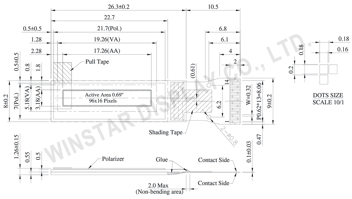
WEO009616B 型號是消費規格小尺吋 COG OLED 顯示器,對角線尺寸0.69吋,解析度96x16像素。此OLED模組內建SSD1306 IC支援I2C傳輸介面,邏輯電源電壓3V (VDD),顯示器電源電壓7.5V (VCC),50%顯示畫面耗電流5mA @7.5V VCC (典型值),驅動方式1/16。此型號OLED模組可支援內部升壓及外部供電。
WEO009616B是一款超薄、輕量、低功耗的小尺寸COG OLED顯示器,非常適合於智能家居應用、醫療設備、手持式裝置、穿戴裝置等,工作溫度範圍在-30℃~+70℃; 儲存溫度範圍為在-30℃~+70℃。
| 項目 | 尺寸 | 單位 |
|---|---|---|
| 點陣 | 96 × 16 Dots | - |
| 模組尺寸 | 26.3 × 8.0 × 1.26 | mm |
| 有效區域 | 17.26 × 3.18 | mm |
| 點大小 | 0.16 × 0.18 | mm |
| 點間距 | 0.18 × 0.20 | mm |
| 顯示模式 | 被動矩陣 | |
| 發光顏色 | 單色 | |
| 驅動方式 | 1/16 Duty | |
| IC | SSD1306 | |
| 介面 | I2C | |
| 尺寸 | 0.69 吋 | |
| 參數 | 符號 | 最小值 | 最大值 | 單位 |
|---|---|---|---|---|
| 邏輯電源電壓 | VDD | 0 | 4 | V |
| 顯示電源電壓 | VCC | 0 | 16 | V |
|
Charge Pump Regulator Supply Voltage |
VBAT | 0 | 5 | V |
| 工作溫度 | TOP | -30 | 70 | °C |
| 儲存溫度 | TSTG | -30 | 70 | °C |
| 項目 | 符號 | 條件 | 最小值 | 典型值 | 最大值 | 單位 |
|---|---|---|---|---|---|---|
| 邏輯電源電壓 | VDD | - | 1.65 | 3.0 | 3.3 | V |
| 顯示電源電壓 (Supplied Externally) | VCC | - | 6.0 | 7.5 | 8.0 | V |
| Charge Pump Regulator Supply Voltage | VBAT | - | 3.0 | - | 4.2 | V |
| Charge Pump Output Voltage for Display (Generated by Internal DC/DC) | Charge Pump VCC |
- | 7.0 | 7.5 | - | V |
| 輸入高電壓. | VIH | - | 0.8×VDD | - | VDD | V |
| 輸入低電壓. | VIL | - | 0 | - | 0.2×VDD | V |
| 輸出高電壓. | VOH | - | 0.9×VDD | - | VDD | V |
| 輸出低電壓. | VOL | - | 0 | - | 0.1×VDD | V |
| 50% 顯示畫面耗電流 (VCC Supplied Externally) | ICC | - | - | 5 | 10 | mA |
| 50% 顯示畫面耗電流 (VCC Generated by Internal DC/DC) | IBAT | - | 5 | 10 | mA |
| No. | 符號 | 說明 |
|---|---|---|
| 1 | C2N | C1P/C1N – Pin for charge pump capacitor; Connect to each other with a capacitor. C2P/C2N – Pin for charge pump capacitor; Connect to each other with a capacitor. |
| 2 | C2P | |
| 3 | C1P | |
| 4 | C1N | |
| 5 | VBAT | This is the power supply pin for the internal buffer of the DC/DC voltage converter. It must be connected to external source when the converter is used. It should be connected to VDD when the converter is not used. |
| 6 | NC | No connection |
| 7 | VSS | This is a ground pin. |
| 8 | VDD | Power supply pin for core logic operation. |
| 9 | RES# | This pin is reset signal input. When the pin is low, initialization of the chip is executed. Keep this pin HIGH (i.e. connect to VDD) during normal operation. |
| 10 | SCL | When I2C mode is selected, D2, D1 should be tied together and serve as SDAout, SDAin in application and D0 is the serial clock input, SCL. |
| 11 | SDA | |
| 12 | IREF | This pin is segment current reference pin. A resistor should be connected between this pin and VSS. Set the current lower than 30uA. When internal IREF is used, this pin should be kept NC. |
| 13 | VCOMH | The pin for COM signal deselected voltage level. A capacitor should be connected between this pin and VSS. |
| 14 | VCC | This is the most positive voltage supply pin of the chip. A stabilization capacitor should be connected between this pin and VSS when the converter is used. It must be connected to external source when the converter is not used. |

通過點擊「允許所有 Cookie」,代表您同意在您的設備上存儲 Cookie 以增強網站瀏覽體驗、分析網站使用情況並協助我們的行銷和網站效能優化工作。您可以在我們的隱私權政策中找到有關於此的更多資訊。