
 - WF57WTLECDNN0")
우리는 귀하의 프라이버시를 소중히 여깁니다
"모든 쿠키 허용"을 클릭하면 사이트 탐색을 개선하고, 사이트 사용을 분석하며, 마케팅 및 성능 노력에 도움을 주기 위해 쿠키를 귀하의 장치에 저장하는 데 동의한 것으로 간주됩니다. 이 주제에 대한 추가 정보는 당사의 정책에서 확인할 수 있습니다. 개인정보 보호정책


WEO009616B E는 0.69인치COG OLED 디스플레이 모듈로, 해상도 96x16픽셀 구성입니다. 이 제품에는 SSD1306 컨트롤러 IC가 기본 내장되어 있으며, I2C 인터페이스, 3V 전력 공급장치를 지원합니다, 대비(일반값)는 10,000:1입니다. 이 모듈 시리즈의 작동 온도는 -30℃에서 +70℃이며, 보관 온도 범위는 -30℃에서 +70℃입니다.
이 모듈은 초박형의 소형 경량 COG OLED 디스플레이로, 전력 소모량도 적습니다. 스마트홈 가전, 의료 기기, 휴대용 디바이스, 웨어러블 디바이스 등에 매우 적합합니다.
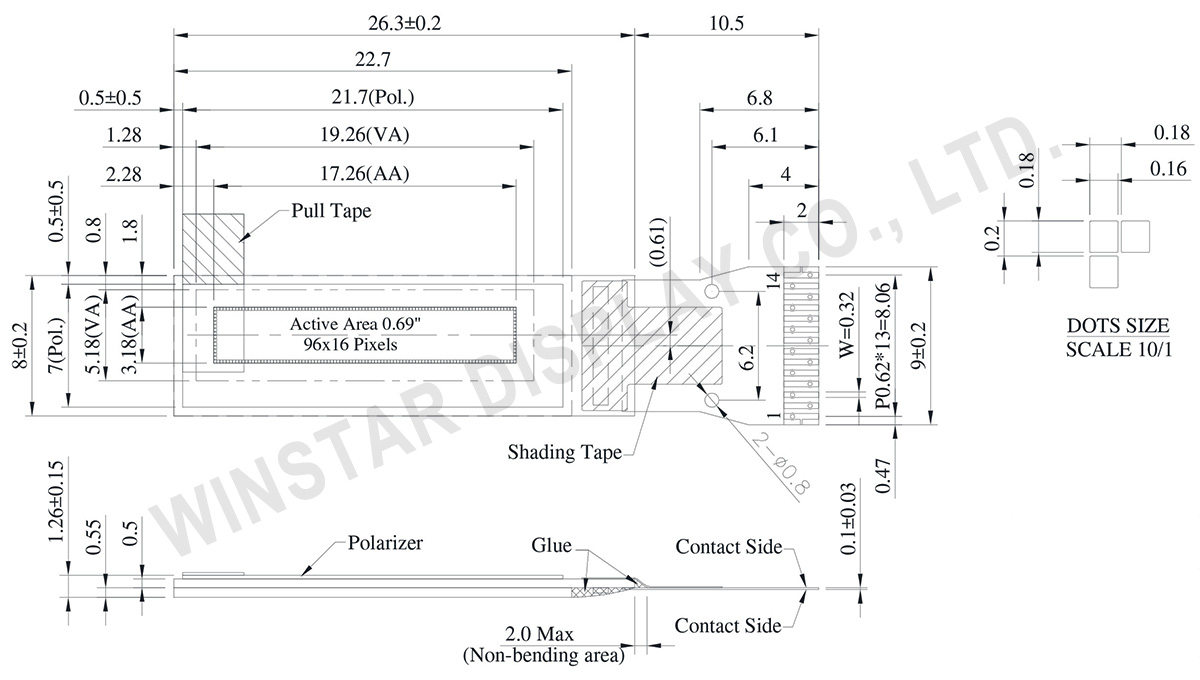
| 항목 | 치수 | 단위 |
|---|---|---|
| 도트 매트릭스 | 96 x 16 점 | - |
| 모듈 치수 | 26.3 × 8.0 × 1.26 | mm |
| 활성 영역 | 17.26 × 3.18 | mm |
| 도트 크기 | 0.16 × 0.18 | mm |
| 도트 피치 | 0.18 × 0.20 | mm |
| 디스플레이 모드 | 패시브 매트릭스 | |
| 디스플레이 색상 | Monochrome | |
| Drive Duty | 1/16 Duty | |
| IC | SSD1306 | |
| 인터페이스 | I2C | |
| 크기 (대각선) | 0.69 인치 | |
| Parameter | 기호 | 최소값 | 최대값 | 단위 |
|---|---|---|---|---|
| Supply Voltage for Logic | VDD | 0 | 4 | V |
| Supply Voltage for Display | VCC | 0 | 16 | V |
|
Charge Pump Regulator Supply Voltage |
VBAT | 0 | 5 | V |
| 작동 온도 | TOP | -30 | 70 | °C |
| 보관 온도 | TSTG | -30 | 70 | °C |
| 항목 | 기호 | 조건 | 최소값 | 대표값 | 최대값 | 단위 |
|---|---|---|---|---|---|---|
| Supply Voltage for Logic | VDD | - | 1.65 | 3.0 | 3.3 | V |
| Supply Voltage for Display (Supplied Externally) |
VCC | - | 6.0 | 7.5 | 8.0 | V |
| Charge Pump Regulator Supply Voltage | VBAT | - | 3.0 | - | 4.2 | V |
| Charge Pump Output Voltage for Display (Generated by Internal DC/DC) | Charge Pump VCC |
- | 7.0 | 7.5 | - | V |
| Input High Volt. | VIH | - | 0.8×VDD | - | VDD | V |
| Input Low Volt. | VIL | - | 0 | - | 0.2×VDD | V |
| Output High Volt. | VOH | - | 0.9×VDD | - | VDD | V |
| Output Low Volt. | VOL | - | 0 | - | 0.1×VDD | V |
| 50% check Board operating Current (VCC Supplied Externally) |
ICC | - | - | 5 | 10 | mA |
| 50% check Board operating Current (VCC Generated by Internal DC/DC) | IBAT | - | 5 | 10 | mA |
| No. | 기호 | 기능 |
|---|---|---|
| 1 | C2N | C1P/C1N – Pin for charge pump capacitor; Connect to each other with a capacitor. C2P/C2N – Pin for charge pump capacitor; Connect to each other with a capacitor. |
| 2 | C2P | |
| 3 | C1P | |
| 4 | C1N | |
| 5 | VBAT | This is the power supply pin for the internal buffer of the DC/DC voltage converter. It must be connected to external source when the converter is used. It should be connected to VDD when the converter is not used. |
| 6 | NC | No connection |
| 7 | VSS | This is a ground pin. |
| 8 | VDD | Power supply pin for core logic operation. |
| 9 | RES# | This pin is reset signal input. When the pin is low, initialization of the chip is executed. Keep this pin HIGH (i.e. connect to VDD) during normal operation. |
| 10 | SCL | When I2C mode is selected, D2, D1 should be tied together and serve as SDAout, SDAin in application and D0 is the serial clock input, SCL. |
| 11 | SDA | |
| 12 | IREF | This pin is segment current reference pin. A resistor should be connected between this pin and VSS. Set the current lower than 30uA. When internal IREF is used, this pin should be kept NC. |
| 13 | VCOMH | The pin for COM signal deselected voltage level. A capacitor should be connected between this pin and VSS. |
| 14 | VCC | This is the most positive voltage supply pin of the chip. A stabilization capacitor should be connected between this pin and VSS when the converter is used. It must be connected to external source when the converter is not used. |

"모든 쿠키 허용"을 클릭하면 사이트 탐색을 개선하고, 사이트 사용을 분석하며, 마케팅 및 성능 노력에 도움을 주기 위해 쿠키를 귀하의 장치에 저장하는 데 동의한 것으로 간주됩니다. 이 주제에 대한 추가 정보는 당사의 정책에서 확인할 수 있습니다. 개인정보 보호정책