 - WL0F00039000QGAAASA00")
我们重视您的隐私
通过点击「允许所有 Cookie」,代表您同意在您的设备上存储 Cookie 以增强网站浏览体验、分析网站使用情况并协助我们的营销和网站效能优化工作。您可以在我们的隐私权政策中找到有关于此的更多信息。


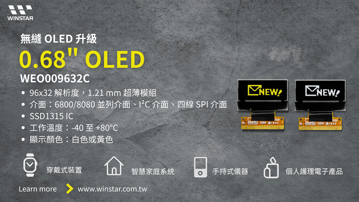
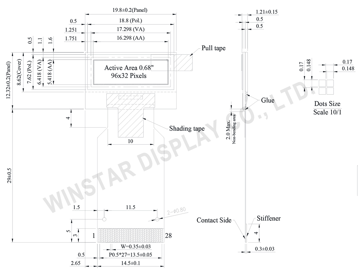
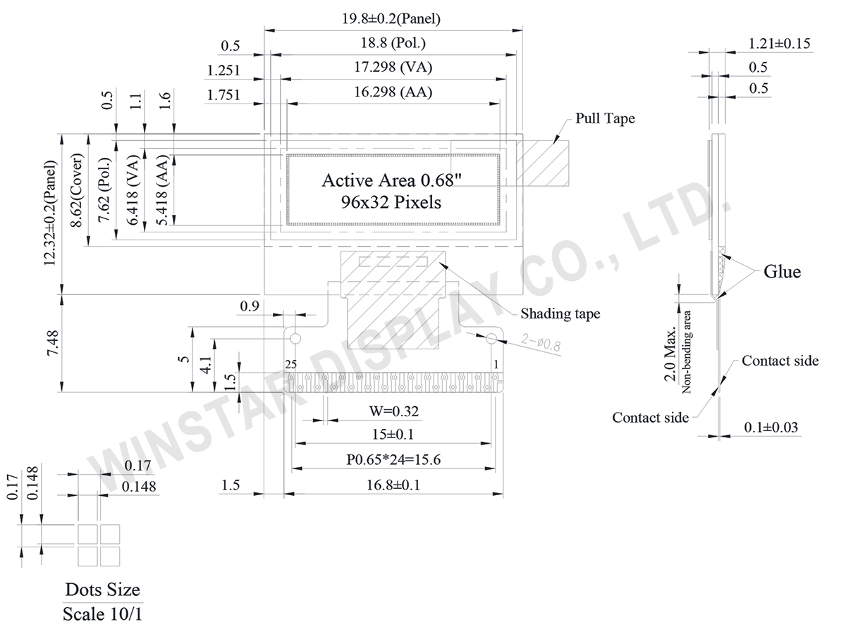
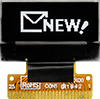
WEO009632C是一款0.68寸微小型的COG OLED显示器模块,分辨率96x32像素。此款模块内建SSD1315 IC,模块操作支持 6800/8080 8-bit 并行接口,I2C与4-线SPI接口,3V电压驱动,1/32 duty,以棋盘格50%画素点亮画面测试,VCC用12V点亮时耗电流3.6mA。此款0.68吋COG结构的 WEO009632C模块工作温度是-40℃至 +80℃,储存温度-40℃至 +85℃。此型号有 ZIF FPC 与 Hotbar FPC 可选择。
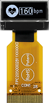
WEO009632C是微小型尺寸COG结构的PMOLED显示器,无需背光非常轻薄,低耗电流,非常适用于穿戴式装置、智能家电、可携带式装置、量测仪器、智能医疗产品、个人健康守护追踪装置等产品。
 可选 FPC
| 项目 | 规格 | 单位 |
|---|---|---|
| 分辨率 | 96 × 32 | Dots |
| 模块尺寸 | 19.80 × 12.32 × 1.21 | mm |
| 有效区域 | 16.298 × 5.418 | mm |
| 像素大小 | 0.148 × 0.148 | mm |
| 像素间距 | 0.17 × 0.17 | mm |
| 显示模式 | 被动矩阵 | |
| 发光颜色 | 单色 | |
| 驱动方式 | 1/32 Duty | |
| IC | SSD1315 | |
| 界面 | 6800, 8080,4-Wire SPI, I2C | |
| 尺寸 | 0.68 吋 | |
| 参数 | 符号 | 最小值 | 典型值 | 最大值 | 单位 |
|---|---|---|---|---|---|
| 逻辑电源电压 | VDD | -0.3 | - | 4 | V |
| 显示电源电压 | VCC | 0 | - | 18 | V |
| 工作温度 | TOP | -40 | - | +80 | °C |
| 储存温度 | TSTG | -40 | - | +85 | °C |
| 项目 | 符号 | 条件 | 最小值 | 典型值 | 最大值 | 单位 |
|---|---|---|---|---|---|---|
| 逻辑电源电压 | VDD | - | 1.65 | 3.0 | 3.3 | V |
| 显示电源电压 | VCC | - | 7.5 | 12.0 | 12.5 | V |
| 输入高准位 | VIH | - | 0.8×VDD | - | VDD | V |
| 输入低准位 | VIL | - | 0 | - | 0.2×VDD | V |
| 输出高准位 | VOH | Iout = 100uA | 0.9×VDD | - | VDD | V |
| 输出低准位 | VOL | Iout = 100uA | 0 | - | 0.1×VDD | V |
| Display 50% Pixel on | ICC | VCC=12V | - | 5.0 | 7.5 | mA |
| No. | 符号 | 功能 | ||||||||||
|---|---|---|---|---|---|---|---|---|---|---|---|---|
| 1 | VSS | Ground pin. It must be connected to external ground. | ||||||||||
| 2 | NC | No connection | ||||||||||
| 3 | VDD | Power supply pin for core logic operation. | ||||||||||
| 4~8 | NC | No connection | ||||||||||
| 9 | VDD | Power supply pin for core logic operation. | ||||||||||
| 10 | BS1 | MCU bus interface selection pins. Select appropriate logic setting as described in the following table. BS2, BS1 are pin select
(1) 0 is connected to VSS (2) 1 is connected to VDD |
||||||||||
| 11 | BS2 | |||||||||||
| 12 | NC | No connection | ||||||||||
| 13 | CS# | This pin is the chip select input connecting to the MCU. The chip is enabled for MCU communication only when CS# is pulled LOW (active LOW). |
||||||||||
| 14 | RES# | This pin is reset signal input. When the pin is pulled LOW, initialization of the chip is executed. Keep this pin HIGH (i.e. connect to VDD) during normal operation. | ||||||||||
| 15 | D/C# | This pin is Data/Command control pin connecting to the MCU. When the pin is pulled HIGH, the data at D[7:0] will be interpreted as data. When the pin is pulled LOW, the data at D[7:0] will be transferred to a command register. In I2C mode, this pin acts as SA0 for slave address selection. |
||||||||||
| 16 | W/R# | This is read / write control input pin connecting to the MCU interface. When interfacing to a 6800-series microprocessor, this pin will be used as Read/Write (R/W#) selection input. Read mode will be carried out when this pin is pulled HIGH (i.e. connect to VDD) and write mode when LOW. When 8080 interface mode is selected, this pin will be the Write (WR#) input. Data write operation is initiated when this pin is pulled LOW and the chip is selected. When serial or I2C interface is selected, this pin must be connected to VSS. |
||||||||||
| 17 | E/RD# | This pin is MCU interface input. When 6800 interface mode is selected, this pin will be used as the Enable (E) signal. Read/write operation is initiated when this pin is pulled HIGH and the chip is selected. When 8080 interface mode is selected, this pin receives the Read (RD#) signal. Read operation is initiated when this pin is pulled LOW and the chip is selected. When serial or I2C interface is selected, this pin must be connected to VSS. |
||||||||||
| 18 | D0 | These are 8-bit bi-directional data bus to be connected to the microprocessor’s data bus. When serial interface mode is selected, D0 will be the serial clock input: SCLK; D1 will be the serial data input: SDIN. When I2C mode is selected, D2, D1 should be tied together and serve as SDAout, SDAin in application and D0 is the serial clock input, SCL. |
||||||||||
| 19 | D1 | |||||||||||
| 20 | D2 | |||||||||||
| 21 | D3 | |||||||||||
| 22 | D4 | |||||||||||
| 23 | D5 | |||||||||||
| 24 | D6 | |||||||||||
| 25 | D7 | |||||||||||
| 26 | IREF | This is segment output current reference pin. When external IREF is used, a resistor should be connected between this pin and VSS to maintain the IREF current at 30uA. |
||||||||||
| 27 | VCOMH | COM signal deselected voltage level. A capacitor should be connected between this pin and VSS. |
||||||||||
| 28 | VCC | Power supply for panel driving voltage. This is also the most positive power voltage supply pin. |
| Drawing | FPC Length | PIN | pitch | ZIF FPC or HOTBAR FPC | Interface | FPC No. | Create Date |
|---|---|---|---|---|---|---|---|
 |
30 | 28 | 0.5 | ZIF FPC | 6800, 8080,4-Wire SPI, I2C | FPC2050002811XXXXX01 | 20180131 |
 |
8.479 | 25 | 0.65 | HOTBAR FPC | 6800, 8080,4-Wire SPI, I2C | FPC2065002501XXXXX00 | 20190906 |

通过点击「允许所有 Cookie」,代表您同意在您的设备上存储 Cookie 以增强网站浏览体验、分析网站使用情况并协助我们的营销和网站效能优化工作。您可以在我们的隐私权政策中找到有关于此的更多信息。