


我们重视您的隐私
通过点击「允许所有 Cookie」,代表您同意在您的设备上存储 Cookie 以增强网站浏览体验、分析网站使用情况并协助我们的营销和网站效能优化工作。您可以在我们的隐私权政策中找到有关于此的更多信息。


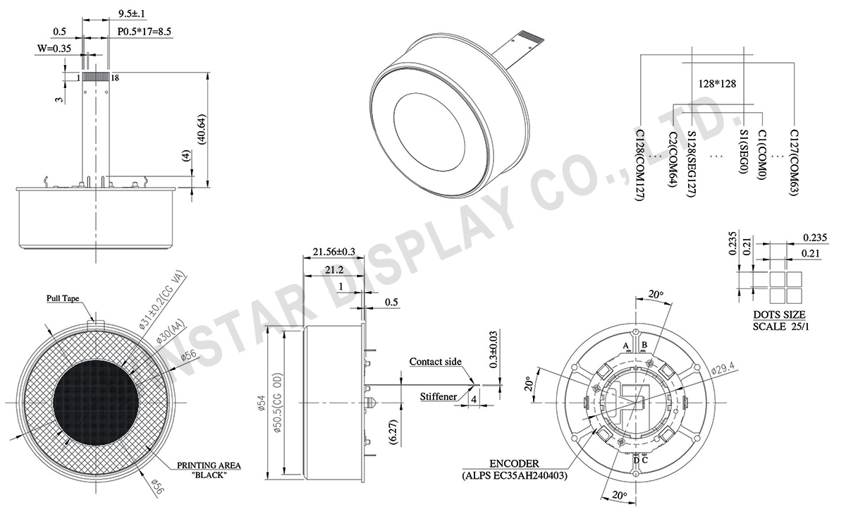
型号 WEO128128D-CTP-Knob
►圆形OLED
►类型:点阵图形
►结构:COG
►尺寸:1.18寸
►128x128点阵
►IC:SSD1327
►3V电源电压
►1/128 duty
►接口:SPI, I2C
►电容式触控面板(CTP)
►支援指数: 1指
►发光颜色: 白色 / 黄色
►支持灰度
WEO128128D型号为圆形OLED加CTP所推出的旋钮样式半成品,是一款有效区域直径Ø1.18吋,分辨率128x128像素的COG OLED。模块内置 SSD1327 IC 支持4线SPI和I2C接口,Typical 逻辑电压为3V,1/128 driving duty。 模块上触控面板内置 FT3268 IC支持I2C接口和一指触控。此型号圆形OLED 非常适合需电容式触控和旋钮进行控制的产品项目使用,例如: 智能家居应用、智能技术设备、影音系统...等。模块工作温度-20℃~+50℃; 储存温度为-30℃~+70℃。
| 项目 | 尺寸 | 单位 |
|---|---|---|
| 点阵(分辨率) | 128 x 128 | Dots |
| 模块尺寸 | Ø56 × 21.56 | mm |
| 检视区域 | Ø30.0 | mm |
| 点大小 | 0.210 × 0.210 | mm |
| 点间距 | 0.235 × 0.235 | mm |
| 显示模式 | 被动矩阵 | |
| 发光颜色 | 单色 | |
| 驱动方式 | 1/128 Duty | |
| 灰阶 | 4 bits | |
| IC | SSD1327 | |
| 接口 | 4线SPI , I2C | |
| 尺寸 | 1.18寸 | |
| CTP IC | FT3268 |
| 检测点(触控点) | 1 |
| CTP 接口 | I2C |
| 参数 | 符号 | 最小值 | 最大值 | 单位 |
|---|---|---|---|---|
| 工作电源电压 | VCI | -0.3 | 3.6 | V |
| 逻辑电源电压 | VDD | -0.5 | 2.75 | V |
| 显示电源电压 | VCC | -0.5 | 19.0 | V |
| 工作温度 | TOP | -20 | +70 | °C |
| 储存温度 | TSTG | -30 | +70 | °C |
| 项目 | 符号 | 条件 | 最小值 | 典型值 | 最大值 | 单位 |
|---|---|---|---|---|---|---|
| 工作电源电压 | VCI | - | 2.8 | 3.0 | 3.3 | V |
| 显示电源电压 | VCC | - | 8.0 | 14.5 | 15.0 | V |
| 逻辑电源电压 | VDD | - | 1.65 | - | 2.6 | V |
| 输入高准位 | VIH | - | 0.8×VCI | - | VCI | V |
| 输入低准位 | VIL | - | 0 | - | 0.2×VCI | V |
| 输出高准位 | VOH | Iout = 100uA | 0.9×VCI | - | VCI | V |
| 输出低准位 | VOL | Iout = 100uA | 0 | - | 0.1×VCI | V |
| 50%显示画面耗电流 | VCC =14.5V | - | 15 | 30 | mA | |
| 项目 | 符号 | 条件 | 最小值 | 典型值 | 最大值 | 单位 |
|---|---|---|---|---|---|---|
| 输入高准位 | VIH | - | 0.7×VDD | - | VDD | V |
| 输入低准位 | VIL | - | -0.3 | - | 0.3×VDD | V |
| 输出高准位 | VOH | IOH = 0.1mA | 0.7×VDD | - | - | V |
| 输出低准位 | VOL | IOL = 0.1mA | - | - | 0.3×VDD | V |
| No. | 符号 | 功能说明 | ||||||
|---|---|---|---|---|---|---|---|---|
| 1 | VSS | Ground pin. It must be connected to external ground. | ||||||
| 2 | VCC | Power supply for panel driving voltage. This is also the most positive power voltage supply pin. It is supplied by external high voltage source. | ||||||
| 3 | VCOMH | COM signal deselected voltage level. A capacitor should be connected between this pin and VSS. No external power supply is allowed to connect to this pin. |
||||||
| 4 | VCI | Low voltage power supply and power supply for interface logic level. It should match with the MCU interface voltage level and must be connected to external source. VCI must always set to be equivalent to or higher than VDD. |
||||||
| 5 | VDD | Power supply pin for core logic operation. VDD can be supplied externally (within the range of 2.4V to 2.6V) or regulated Internally from VCI. A capacitor should be connected between VDD and VSS under all circumstances. |
||||||
| 6 | BS1 | MCU bus interface selection pins. Select appropriate logic setting as described in the following table. BS1 is pin select. Bus Interface selection
|
||||||
| 7 | IREF | This pin is the segment output current reference pin | ||||||
| 8 | CS# | This pin is the chip select input connecting to the MCU. The chip is enabled for MCU communication only when CS# is pulled LOW (active LOW). |
||||||
| 9 | RES# | This pin is reset signal input. When the pin is pulled LOW, initialization of the chip is executed. Keep this pin pull HIGH during normal operation. |
||||||
| 10 | DC# | This pin is Data/Command control pin connecting to the MCU. When the pin is pulled HIGH, will be interpreted as data. When the pin is pulled LOW, will be transferred to a command register In I2C mode, this pin acts as SA0 for slave address selection. |
||||||
| 11 | D0 | When serial interface mode is selected, D0 will be the serial clock input: SCLK; D1 will be the serial data input: SDIN and D2 should be kept NC. When I2C mode is selected, D2, D1 should be tied together and serve as SDAout , SDAin in application and D0 is the serial clock input, SCL. |
||||||
| 12 | D1 | |||||||
| 13 | D2 | |||||||
| 14 | TP_SCK | I2C clock signal | ||||||
| 15 | TP_SDA | I2C data signal | ||||||
| 16 | TP_INT | Interrupt signal | ||||||
| 17 | VCC | Power supply for panel driving voltage. This is also the most positive power voltage supply pin. | ||||||
| 18 | VSS | Ground |
| No. | 符号 | 功能说明 |
|---|---|---|
| 1 | FSW_A | Encoder terminal signal-A |
| 2 | FSW_B | Encoder terminal signal-B |
| 3 | FSW_C | Encoder terminal signal-C |
| 4 | FSW_D | Ground |

通过点击「允许所有 Cookie」,代表您同意在您的设备上存储 Cookie 以增强网站浏览体验、分析网站使用情况并协助我们的营销和网站效能优化工作。您可以在我们的隐私权政策中找到有关于此的更多信息。