


私たちはあなたのプライバシーを大切にします
「すべてのクッキーを許可」をクリックすると、サイトのナビゲーションを向上させ、サイト使用状況を分析し、マーケティングおよびパフォーマンスの取り組みを支援するために、クッキーをデバイスに保存することに同意したことになります。この件に関する詳細情報は、ポリシーをご覧ください。プライバシーポリシー


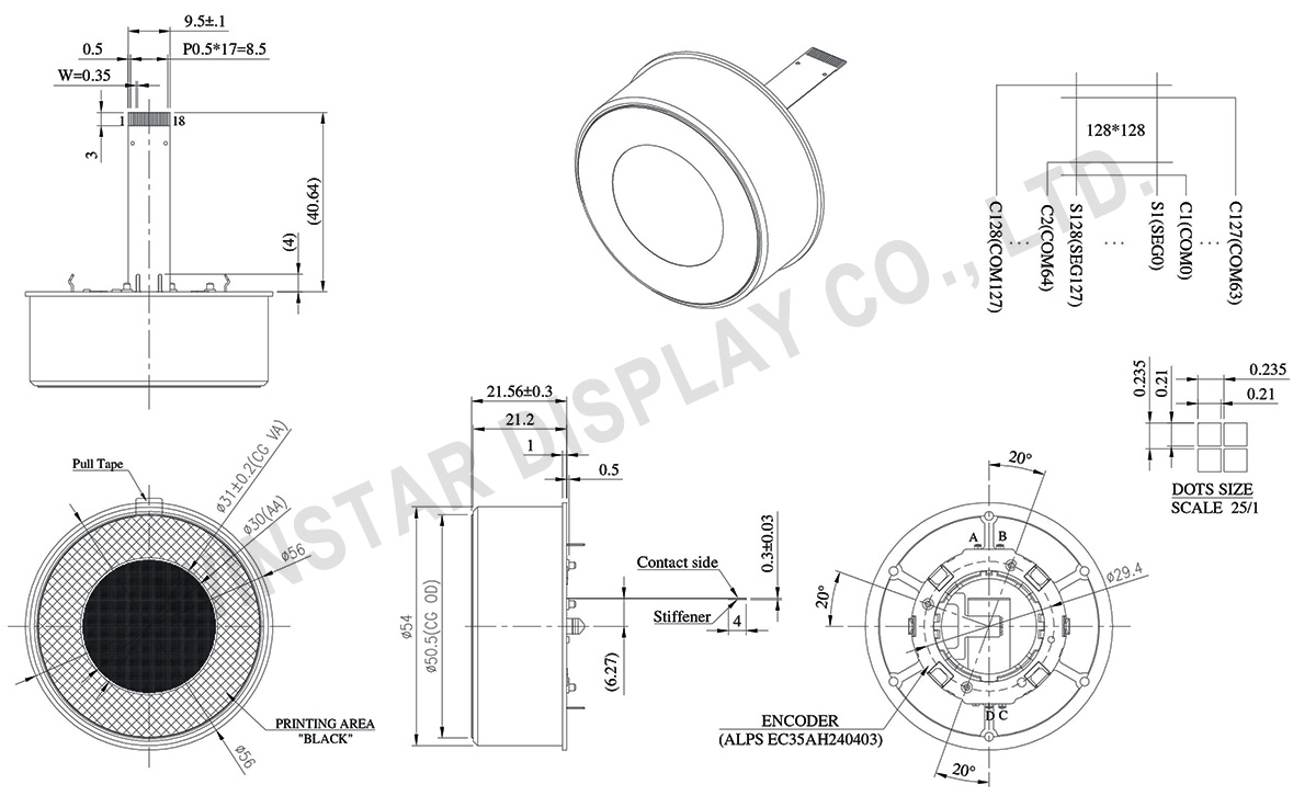
型番 WEO128128D-CTP-Knob
►ノブ付き円形OLED
►グラフィック有機ELモジュール
►結構: COG
►サイズ:1.18インチ
►128x128 ドットマトリックス
►IC:SSD1327
►3V電源電圧
►1/128 duty
►インターフェース: SPI, I2C
►静電容量式タッチパネル(CTP)
►検出ポイント: 1
►発光色: 白色 / 黄色
►グレースケール機能をサポートする
円型OLEDWEO128128D-CTP ノブ付きモデルは、静電容量式タッチスクリーンとモジュールのコントロールノブを備えた拡張アイテムで、それはØ1.18インチの円形COGタイプOLEDディスプレイで、解像度128x128ドットで作られて、このモジュールはSSD1327 ICに組み込まれております。4ラインSPI及びI2Cインターフェースをサポートします。ロジック3Vの供給電圧(標準値)で、駆動デューティ1/128です。このモジュールはFT3268タッチパネルICに組み込まれて、1本の指でポイントを検出して、I2Cインターフェイスをサポートします。
静電容量式タッチスクリーンとノブを備えたこの丸いOLEDから拡張したWEO128128Dモデルは、スマートホームアプリケーション、インテリジェントテクノロジーデバイス、オーディオシステムなどのデバイスにコントロールノブが必要なアプリケーションに最適です。操作温度範囲は-20℃から+50℃で、保存温度範囲は-30℃から+70℃です。
| 項目 | サイズ | 単位 |
|---|---|---|
| ドットマトリックス(解像度) | 128 x 128 | Dots |
| モジュールサイズ | Ø56 × 21.56 | mm |
| 有効エリア | Ø30.0 | mm |
| ドットサイズ | 0.210 × 0.210 | mm |
| ドットピッチ | 0.235 × 0.235 | mm |
| 表示モード | パッシブマトリクス | |
| 表示カラー | モノクロ | |
| 駆動方法 | 1/128Duty | |
| グレースケール | 4 bits | |
| IC | SSD1327 | |
| インターフェイス | 4-line SPI , I2C | |
| サイズ(対角線) | 1.18インチ | |
| CTP IC | FT3268 |
| 検出ポイント | 1 |
| CTP インターフェイス | I2C |
| パラメーター | 記号 | 最小値 | 最大値 | 単位 |
|---|---|---|---|---|
| 動作電源電圧 | VCI | -0.3 | 3.6 | V |
| ロジック電源電圧 | VDD | -0.5 | 2.75 | V |
| Display電源電圧 | VCC | -0.5 | 19.0 | V |
| 動作温度 | TOP | -20 | +70 | °C |
| 保存温度 | TSTG | -30 | +70 | °C |
| 項目 | 記号 | 條件 | 最小値 | 典型値 | 最大値 | 単位 |
|---|---|---|---|---|---|---|
| 動作電源電圧 | VCI | - | 2.8 | 3.0 | 3.3 | V |
| Display電源電圧 | VCC | - | 8.0 | 14.5 | 15.0 | V |
| ロジック電源電圧 | VCC | - | 1.65 | - | 2.6 | V |
| 高レベル入力 | VIH | - | 0.8×VCI | - | VCI | V |
| 低レベル入力 | VIL | - | 0 | - | 0.2×VCI | V |
| 高レベル出力 | VOH | Iout = 100uA | 0.9×VCI | - | VCI | V |
| 低レベル出力 | VOL | Iout = 100uA | 0 | - | 0.1×VCI | V |
| 50% Check Board operating Current | VCC =14.5V | - | 15 | 30 | mA | |
| 項目 | 記号 | 條件 | 最小値 | 典型値 | 最大値 | 単位 |
|---|---|---|---|---|---|---|
| 高レベル入力 | VIH | - | 0.7×VDD | - | VDD | V |
| 低レベル入力 | VIL | - | -0.3 | - | 0.3×VDD | V |
| 高レベル出力 | VOH | IOH = 0.1mA | 0.7×VDD | - | - | V |
| 低レベル出力 | VOL | IOL = 0.1mA | - | - | 0.3×VDD | V |
| No. | 記号 | 説明 | ||||||
|---|---|---|---|---|---|---|---|---|
| 1 | VSS | Ground pin. It must be connected to external ground. | ||||||
| 2 | VCC | Power supply for panel driving voltage. This is also the most positive power voltage supply pin. It is supplied by external high voltage source. | ||||||
| 3 | VCOMH | COM signal deselected voltage level. A capacitor should be connected between this pin and VSS. No external power supply is allowed to connect to this pin. | ||||||
| 4 | VCI | Low voltage power supply and power supply for interface logic level. It should match with the MCU interface voltage level and must be connected to external source. VCI must always set to be equivalent to or higher than VDD. | ||||||
| 5 | VDD | Power supply pin for core logic operation. VDD can be supplied externally (within the range of 2.4V to 2.6V) or regulated Internally from VCI. A capacitor should be connected between VDD and VSS under all circumstances. |
||||||
| 6 | BS1 | MCU bus interface selection pins. Select appropriate logic setting as described in the following table. BS1 is pin select. Bus Interface selection
|
||||||
| 7 | IREF | This pin is the segment output current reference pin | ||||||
| 8 | CS# | This pin is the chip select input connecting to the MCU. The chip is enabled for MCU communication only when CS# is pulled LOW (active LOW). | ||||||
| 9 | RES# | This pin is reset signal input. When the pin is pulled LOW, initialization of the chip is executed. Keep this pin pull HIGH during normal operation. | ||||||
| 10 | DC# | This pin is Data/Command control pin connecting to the MCU. When the pin is pulled HIGH, will be interpreted as data. When the pin is pulled LOW, will be transferred to a command register In I2C mode, this pin acts as SA0 for slave address selection. | ||||||
| 11 | D0 | When serial interface mode is selected, D0 will be the serial clock input: SCLK; D1 will be the serial data input: SDIN and D2 should be kept NC. When I2C mode is selected, D2, D1 should be tied together and serve as SDAout , SDAin in application and D0 is the serial clock input, SCL. | ||||||
| 12 | D1 | |||||||
| 13 | D2 | |||||||
| 14 | TP_SCK | I2C clock signal | ||||||
| 15 | TP_SDA | I2C data signal | ||||||
| 16 | TP_INT | Interrupt signal | ||||||
| 17 | VCC | Power supply for panel driving voltage. This is also the most positive power voltage supply pin. | ||||||
| 18 | VSS | Ground |
| No. | 記号 | 説明 |
|---|---|---|
| 1 | FSW_A | Encoder terminal signal-A |
| 2 | FSW_B | Encoder terminal signal-B |
| 3 | FSW_C | Encoder terminal signal-C |
| 4 | FSW_D | Ground |

「すべてのクッキーを許可」をクリックすると、サイトのナビゲーションを向上させ、サイト使用状況を分析し、マーケティングおよびパフォーマンスの取り組みを支援するために、クッキーをデバイスに保存することに同意したことになります。この件に関する詳細情報は、ポリシーをご覧ください。プライバシーポリシー