


私たちはあなたのプライバシーを大切にします
「すべてのクッキーを許可」をクリックすると、サイトのナビゲーションを向上させ、サイト使用状況を分析し、マーケティングおよびパフォーマンスの取り組みを支援するために、クッキーをデバイスに保存することに同意したことになります。この件に関する詳細情報は、ポリシーをご覧ください。プライバシーポリシー


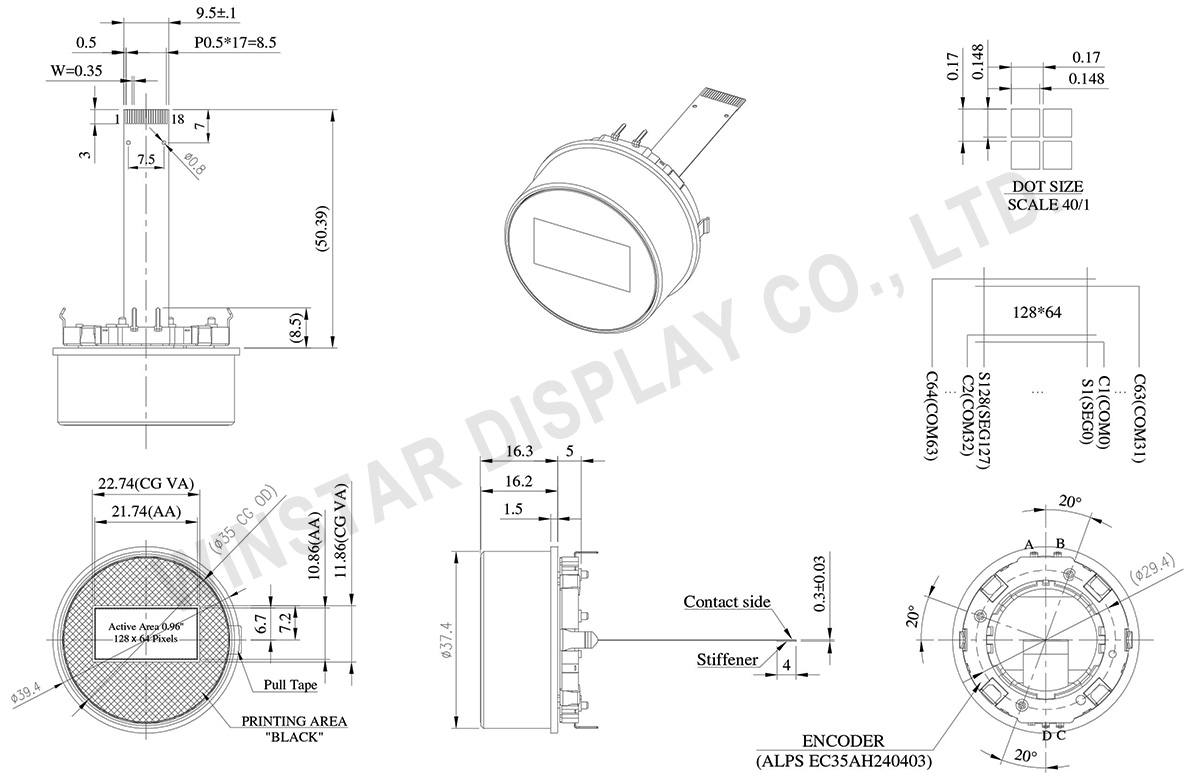
型番 WEO012864Z
►ノブ付き円形OLED
►グラフィック有機ELモジュール
►結構: COG
►サイズ:0.96インチ
►128x64 ドットマトリックス
►IC:SSD1306
►3V電源電圧
►1/64 duty
►インターフェース: SPI, I2C
►発光色: 白色 / 黄色 / 空色
WEO012864Z シリーズOLEDはコントロールノブを備えたWEO012864Dの拡張アイテムで、0.96インチのCOGタイプのOLEDディスプレイです。解像度 128x64 ドットで、 SSD1306 IC を内蔵しております。 4 ライン SPI 及び I2C インターフェースをサポートして、供給電圧 (VCI) 最小 1.65V、最大 3.3Vで、1/64 駆動デューティです。
この WEO012864Z OLED は、スマート ホーム アプリケーション、インテリジェント テクノロジー デバイス、オーディオ システムなどのデバイスのコントロール ノブが必要なアプリケーションに最適なロータリー スイッチを備えております。操作温度範囲は-20℃~+70℃で、 保存温度範囲は-30℃~+80℃です。
Data source ref: WEO012864ZLPP3N00000
| 項目 | サイズ | 単位 |
|---|---|---|
| ドットマトリックス(解像度) | 128 x 64 | Dots |
| モジュールサイズ | Ø39.4 x 24.8 | mm |
| 有効エリア | 21.74 x 10.86 | mm |
| ドットサイズ | 0.148 x 0.148 | mm |
| ドットピッチ | 0.17 x 0.17 | mm |
| 表示モード | パッシブマトリクス | |
| 表示カラー | モノクロ | |
| 駆動方法 | 1/64 | |
| IC | SSD1326 | |
| インターフェイス | 4線 SPI , I2C | |
| サイズ(対角線) | 0.96インチ | |
| 項目 | 記号 | 最小値 | 最大値 | 単位 |
|---|---|---|---|---|
| 電源電圧 | VCI | -0.3 | 4.0 | V |
| Display電源電圧 | VCC | 0 | 15 | V |
| 動作温度 | TOP | -20 | +70 | °C |
| 保存温度 | TST | -30 | +80 | °C |
| 項目 | 記号 | 條件 | 最小値 | 典型値 | 最大値 | 単位 |
|---|---|---|---|---|---|---|
| 電源電圧 | VCI | - | 1.65 | 3.0 | 3.3 | V |
| Display電源電圧 | VCC | - | 6 | 10 | 10.5 | V |
| 高レベル入力 | VIH | - | 0.8xVCI | - | - | V |
| 低レベル入力 | VIL | - | - | - | 0.2xVCI | V |
| 高レベル出力 | VOH | Iout = 100uA | 0.9xVCI | - | - | V |
| 低レベル出力 | VOL | Iout = 100uA | - | - | 0.1xVCI | V |
| VCC動作電流 (VCC Supplied Externally) | ICC | VCC =10V | - | 5 | 10 | mA |
| Pin No. | 記号 | 説明 | ||||||
|---|---|---|---|---|---|---|---|---|
| 1 | VSS | Ground pin. | ||||||
| 2 | VCC | Power supply for panel driving voltage. This is also the most positive power voltage supply pin. | ||||||
| 3 | VCOMH | COM signal deselected voltage level. A capacitor should be connected between this pin and VSS. |
||||||
| 4 | VCI | Power supply pin for core logic operation | ||||||
| 5 | NC | No connection | ||||||
| 6 | BS1 | MCU bus interface selection pins. Select appropriate logic setting as described in the following table.
(1) 0 is connected to VSS (2) 1 is connected to VCI |
||||||
| 7 | IREF | This is segment output current reference pin. When external IREF is used, a resistor should be connected between this pin and VSS to maintain the IREF current at a maximum of 30uA. |
||||||
| 8 | CS# | This pin is the chip select input. (active LOW). | ||||||
| 9 | RES# | This pin is reset signal input. When the pin is pulled LOW, initialization of the chip is executed. Keep this pin HIGH during normal operation. |
||||||
| 10 | D/C# | When 4-wire serial interface is selected, this pin is Data/Command control pin connecting to the MCU. In I2C mode, this pin acts as SA0 for slave address selection. |
||||||
| 11 | D0 | These pins are bi-directional data bus connecting to the MCU data bus. When serial interface mode is selected, D0 will be the serial clock input: SCLK; D1 will be the serial data input: SDIN and D2 should be kept NC. When I2C mode is selected, D2, D1 should be tied together and serve as SDAout, SDAin in application and D0 is the serial clock input, SCL. |
||||||
| 12 | D1 | |||||||
| 13 | D2 | |||||||
| 14 | NC | No connection | ||||||
| 15 | NC | No connection | ||||||
| 16 | NC | No connection | ||||||
| 17 | VCC | Power supply for panel driving voltage. This is also the most positive power voltage supply pin. | ||||||
| 18 | VSS | Ground pin. |
| No. | 記号 | 説明 |
|---|---|---|
| 1 | FSW_A | Encoder terminal signal-A |
| 2 | FSW_B | Encoder terminal signal-B |
| 3 | FSW_C | Encoder terminal signal-C |
| 4 | FSW_D | Ground |

「すべてのクッキーを許可」をクリックすると、サイトのナビゲーションを向上させ、サイト使用状況を分析し、マーケティングおよびパフォーマンスの取り組みを支援するために、クッキーをデバイスに保存することに同意したことになります。この件に関する詳細情報は、ポリシーをご覧ください。プライバシーポリシー