


私たちはあなたのプライバシーを大切にします
「すべてのクッキーを許可」をクリックすると、サイトのナビゲーションを向上させ、サイト使用状況を分析し、マーケティングおよびパフォーマンスの取り組みを支援するために、クッキーをデバイスに保存することに同意したことになります。この件に関する詳細情報は、ポリシーをご覧ください。プライバシーポリシー


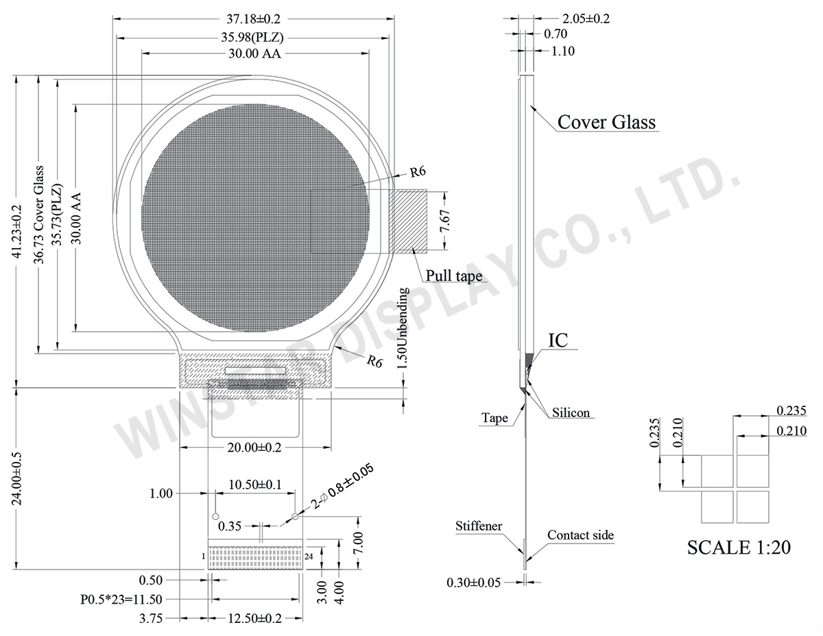
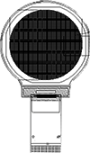
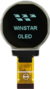
型番 WEO128128B
►円形液晶
►グラフィック有機ELモジュール
►結構: COG
►サイズ:1.18インチ
►128x128 ドットマトリックス
►IC:SSD1327
►3V電源電圧
►1/128 duty
►インターフェース: 6800, 8080, SPI, I2C
►発光色: 白色 / 黄色
►グレースケール機能をサポートする
►Other FPC options available in below table
WEO128128B は1.18インチ 円形 のパッシブマトリックス 駆動有機ELディスプレイです。 解像度が128x128 pixelsです。SSD1327ZB controller ICを内臓して、8bit 6800/8080/3線と4線のSPI/I2Cのインターフェースをサポート致します。3V駆動対応品です。 外形寸法は37.18×41.23×2.05 mmで、AAサイズはØ30 mm です。
WEO128128BはCOG構造する有機ELディスプレイ、それにバックライトが不要(自己発光)です ので、軽量、低消費電力です。この有機ELモジュールはハンドヘルド機器、メーター、IoT、工業制御設備等のアイテムに適しています。 標準的な発光色が黄色ですが、オプションは白とスカイブルーをご利用いただけます。他の表示色が必要な場合、当社の営業担当者にお問い合わせください。 操作温度は-40℃から +80℃までで、保存温度は -40℃から 85℃です。他のお問い合わせがあれば、何卒担当業務にご連絡ください。
 FPC Options
| 項目 | サイズ | 単位 |
|---|---|---|
| ドットマトリックス(解像度) | 128 x 128 | Dots |
| モジュールサイズ | 37.18× 41.23 × 2.05 | mm |
| 有効エリア | Ø30 | mm |
| ドットサイズ | 0.210 × 0.210 | mm |
| ドットピッチ | 0.235 × 0.235 | mm |
| 表示モード | パッシブマトリクス | |
| 表示カラー | モノクロ | |
| 駆動方法 | 1/128Duty | |
| グレースケール | 4 bits | |
| IC | SSD1327 | |
| インターフェイス | 6800, 8080, 4線 SPI, I2C | |
| サイズ(対角線) | 1.18インチ | |
| パラメーター | 記号 | 最小値 | 最大値 | 単位 |
|---|---|---|---|---|
| 低電圧電源,入力/出力ピンの電源電圧 | VCI | -0.3 | 4.0 | V |
| ロジック電源電圧 | VDD | -0.5 | 2.75 | V |
| Display電源電圧 | VCC | -0.5 | 19.0 | V |
| 動作温度 | TOP | -40 | +80 | °C |
| 保存温度 | TSTG | -40 | +85 | °C |
| 項目 | 記号 | 條件 | 最小値 | 典型値 | 最大値 | 単位 |
|---|---|---|---|---|---|---|
| 低電圧電源,入力/出力ピンの電源電圧 | VCI | Note | 2.8 | 3 | 3.3 | V |
| Display電源電圧 | VCC | - | 14 | 14.5 | 15 | V |
| ロジック電源電圧 | VDD | - | 2.4 | - | 2.6 | V |
| 高レベル入力 | VIH | - | 0.8×VCI | - | VCI | V |
| 低レベル入力 | VIL | - | 0 | - | 0.2×VCI | V |
| 高レベル出力 | VOH | - | 0.9×VCI | - | VCI | V |
| 低レベル出力 | VOL | - | 0 | - | 0.1×VCI | V |
| 50% Check Board operating Current | VCC =14.5V | - | 24 | 26 | mA | |
Note: VCI must be larger than or equal to VDD
| No. | 記号 | 説明 | ||||||||||
|---|---|---|---|---|---|---|---|---|---|---|---|---|
| 1 | VSS | Ground pin. It must be connected to external ground. | ||||||||||
| 2 | VCC | Power supply for panel driving voltage. This is also the most positive power voltage supply pin. It is supplied by external high voltage source. | ||||||||||
| 3 | VCOMH | COM signal deselected voltage level. A capacitor should be connected between this pin and VSS. No external power supply is allowed to connect to this pin. |
||||||||||
| 4 | VCI | Low voltage power supply and power supply for interface logic level. It should match with the MCU interface voltage level and must be connected to external source. VCI must always set to be equivalent to or higher than VDD. |
||||||||||
| 5 | VDD | Power supply pin for core logic operation. VDD can be supplied externally (within the range of 2.4V to 2.6V) or regulated Internally from VCI. A capacitor should be connected between VDD and VSS under all circumstances. |
||||||||||
| 6 | BS1 |
MCU bus interface selection pins. Select appropriate logic setting as described in the following table. BS2 and BS1 are pin select.
|
||||||||||
| 7 | BS2 | |||||||||||
| 8 | VSS | Ground pin. It must be connected to external ground. | ||||||||||
| 9 | IREF | This pin is the segment output current reference pin | ||||||||||
| 10 | CS# | This pin is the chip select input connecting to the MCU. The chip is enabled for MCU communication only when CS# is pulled LOW (active LOW). |
||||||||||
| 11 | RES# | This pin is reset signal input. When the pin is pulled LOW, initialization of the chip is executed. Keep this pin pull HIGH during normal operation. |
||||||||||
| 12 | D/C | This pin is Data/Command control pin connecting to the MCU. When the pin is pulled HIGH, the data at D[7:0] will be interpreted as data. When the pin is pulled LOW, the data at D[7:0] will be transferred to a command register. In I2C mode, this pin acts as SA0 for slave address selection. When 3-wire serial interface is selected, this pin must be connected to VSS. |
||||||||||
| 13 | W/R# | This pin is read / write control input pin connecting to the MCU interface. When 6800 interface mode is selected, this pin will be used as Read/Write (R/W#) selection input. Read mode will be carried out when this pin is pulled HIGH and write mode when LOW. When 8080 interface mode is selected, this pin will be the Write (WR#) input. Data write operation is initiated when this pin is pulled LOW and the chip is selected. |
||||||||||
| 14 | RD# | This pin is MCU interface input. When 6800 interface mode is selected, this pin will be used as the Enable (E) signal. Read/write operation is initiated when this pin is pulled HIGH and the chip is selected. When 8080 interface mode is selected, this pin receives the Read (RD#) signal. Read operation is initiated when this pin is pulled LOW and the chip is selected. When serial or I2C interface is selected, this pin must be connected to VSS. |
||||||||||
| 15 | D0 | These pins are bi-directional data bus connecting to the MCU data bus. Unused pins are recommended to tie LOW. When serial interface mode is selected, D0 will be the serial clock input: SCLK; D1 will be the serial data input: SDIN and D2 should be kept NC. When I2C mode is selected, D2, D1 should be tied together and serve as SDAout, SDAin in application and D0 is the serial clock input, SCL. |
||||||||||
| 16 | D1 | |||||||||||
| 17 | D2 | |||||||||||
| 18 | D3 | |||||||||||
| 19 | D4 | |||||||||||
| 20 | D5 | |||||||||||
| 21 | D6 | |||||||||||
| 22 | D7 | |||||||||||
| 23 | VCC | Power supply for panel driving voltage. This is also the most positive power voltage supply pin. It is supplied by external high voltage source. | ||||||||||
| 24 | VSS | Ground pin. |
| Drawing | FPC Length | PIN | Pitch | ZIF / HOTBAR FPC | Interface | FPC No. | Create Date |
|---|---|---|---|---|---|---|---|
 |
25.05 | 24 | 0.5 | ZIF | 6800,8080,SPI,I2C | FPC2050002411XXXXX02 | 20160511 |
 |
91 | 18 | 0.5 | ZIF | 4-line SPI , I2C | FPC2050001811XXXXX04 | 20180705 |

「すべてのクッキーを許可」をクリックすると、サイトのナビゲーションを向上させ、サイト使用状況を分析し、マーケティングおよびパフォーマンスの取り組みを支援するために、クッキーをデバイスに保存することに同意したことになります。この件に関する詳細情報は、ポリシーをご覧ください。プライバシーポリシー