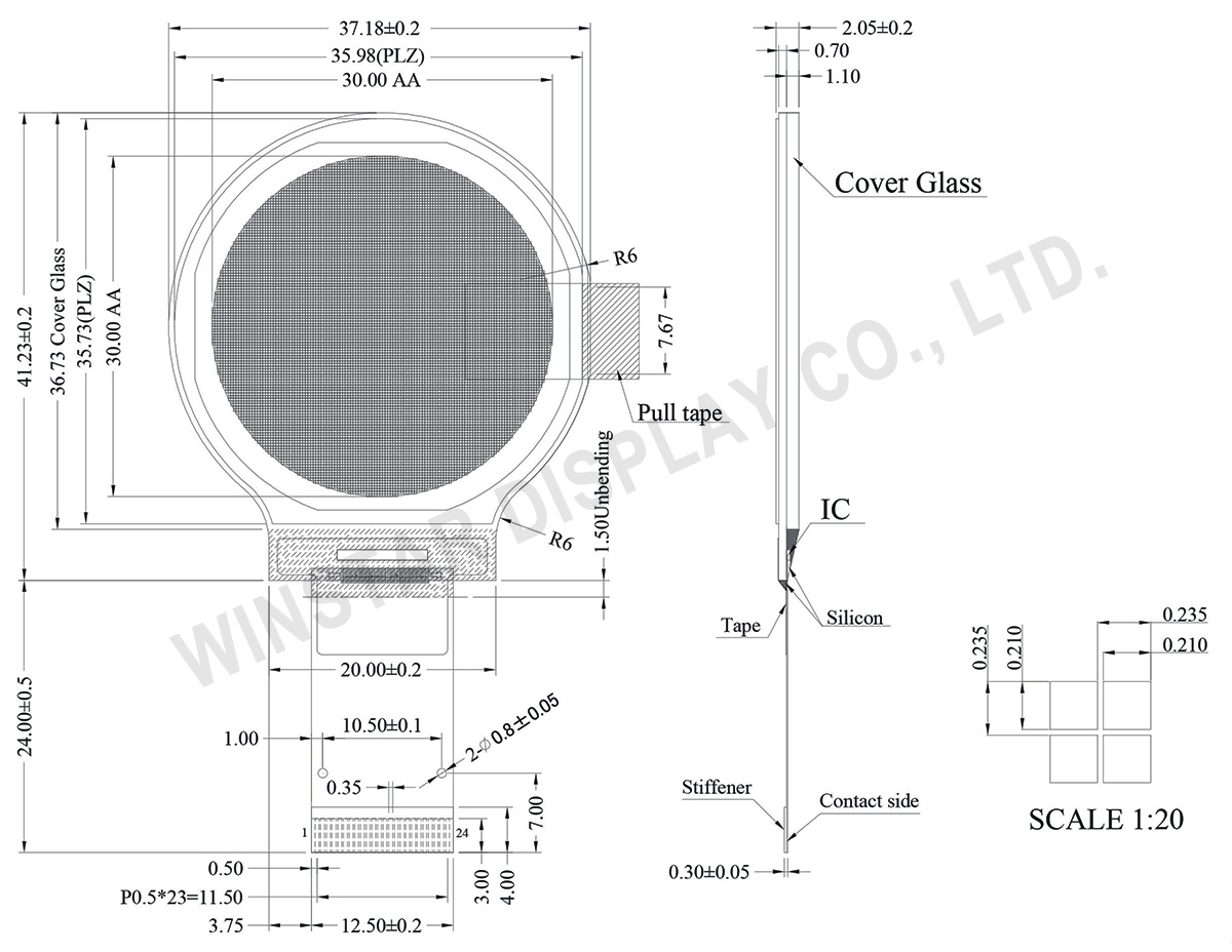
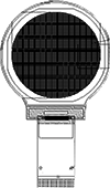
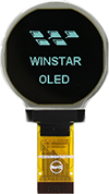
WEO128128B é um Tela display circular OLED COG, resolução de 128x128 pixéis. Este módulo tem dimensão de módulo de 37,18 x 41,23 mm e área ativa de Ø1,18". Este display OLED está integrado com o IC SSD1327, suporta interface 6800, 8080, SPI 4 fios e I2C. 1/128 duty, suporte em escala de cinza.
A tensão de alimentação para lógica (VDD) é de 2,8V a 3,3V, valor típico de 3,0V, relação de contraste (valor típico) de 2,000:1. Esta série de módulos pode operar a temperaturas de -40℃ a +80℃; suas temperaturas de armazenamento variam de -40℃ a +85℃.
Este módulo é um display COG OLED de circular, ultra-fino, leve e com baixo consumo de energia. Ele é muito adequado para aplicações domésticas inteligentes, dispositivos de tecnologia inteligente, sistema de áudio, etc.
Low voltage power supply, power supply for I/O pins
VCI
-0.3
4.0
V
Supply Voltage for Logic
VDD
-0.5
2.75
V
Supply Voltage for Display
VCC
-0.5
19.0
V
Temperatura de operação
TOP
-40
+80
°C
Temperatura de armazenamento
TSTG
-40
+85
°C
Características Eletrônicas
DC Características Eletrônicas
Item
Símbolo
Condição
Valor Min
Valor Típico
Valor Máximo
Unidade
Low voltage power supply, power supply for I/O pins
VCI
Note
2.8
3.0
3.3
V
Supply Voltage for Display
VCC
-
14
14.5
15
V
Supply Voltage for Logic
VDD
-
2.4
-
2.6
V
High Level Input
VIH
-
0.8×VCI
-
VCI
V
Low Level Input
VIL
-
0
-
0.2×VCI
V
High Level Output
VOH
-
0.9×VCI
-
VCI
V
Low Level Output
VOL
-
0
-
0.1×VCI
V
50% Check Board operating Current
VCC =14.5V
-
24
26
mA
Note: VCI must be larger than or equal to VDD
Função do pino de interface
No.
Símbolo
Função
1
VSS
Ground pin. It must be connected to external ground.
2
VCC
Power supply for panel driving voltage. This is also the most positive power voltage supply pin. It is supplied by external high voltage source.
3
VCOMH
COM signal deselected voltage level.
A capacitor should be connected between this pin and VSS. No external power supply is allowed to connect to this pin.
4
VCI
Low voltage power supply and power supply for interface logic level. It should match with the MCU interface voltage level and must be connected to external source.
VCI must always set to be equivalent to or higher than VDD.
5
VDD
Power supply pin for core logic operation.
VDD can be supplied externally (within the range of 2.4V to 2.6V) or regulated
Internally from VCI. A capacitor should be connected between VDD and VSS under all circumstances.
6
BS1
MCU bus interface selection pins. Select appropriate logic setting as described in the following table. BS2 and BS1 are pin select.
Bus Interface selection
BS[2:1]
Interface
0
4 line SPI
1
I2C
11
8-bit 8080 parallel
10
8-bit 6800 parallel
Note (1) 0 is connected to VSS (2) 1 is connected to VCI
7
BS2
8
VSS
Ground pin. It must be connected to external ground.
9
IREF
This pin is the segment output current reference pin
10
CS#
This pin is the chip select input connecting to the MCU.
The chip is enabled for MCU communication only when CS# is pulled LOW (active LOW).
11
RES#
This pin is reset signal input.
When the pin is pulled LOW, initialization of the chip is executed.
Keep this pin pull HIGH during normal operation.
12
D/C
This pin is Data/Command control pin connecting to the MCU.
When the pin is pulled HIGH, the data at D[7:0] will be interpreted as data.
When the pin is pulled LOW, the data at D[7:0] will be transferred to a command register.
In I2C mode, this pin acts as SA0 for slave address selection.
When 3-wire serial interface is selected, this pin must be connected to VSS.
13
W/R#
This pin is read / write control input pin connecting to the MCU interface.
When 6800 interface mode is selected, this pin will be used as Read/Write (R/W#) selection input. Read mode will be carried out when this pin is pulled HIGH and write mode when LOW.
When 8080 interface mode is selected, this pin will be the Write (WR#) input. Data write operation is initiated when this pin is pulled LOW and the chip is selected.
14
RD#
This pin is MCU interface input.
When 6800 interface mode is selected, this pin will be used as the Enable (E) signal.
Read/write operation is initiated when this pin is pulled HIGH and the chip is selected.
When 8080 interface mode is selected, this pin receives the Read (RD#) signal. Read operation is initiated when this pin is pulled LOW and the chip is selected.
When serial or I2C interface is selected, this pin must be connected to VSS.
15
D0
These pins are bi-directional data bus connecting to the MCU data bus.
Unused pins are recommended to tie LOW.
When serial interface mode is selected, D0 will be the serial clock input: SCLK; D1 will be the serial data input: SDIN and D2 should be kept NC.
When I2C mode is selected, D2, D1 should be tied together and serve as SDAout, SDAin in application and D0 is the serial clock input, SCL.
16
D1
17
D2
18
D3
19
D4
20
D5
21
D6
22
D7
23
VCC
Power supply for panel driving voltage. This is also the most positive power voltage supply pin. It is supplied by external high voltage source.
Ao clicar em "Permitir todos os cookies", você concorda com o armazenamento de cookies no seu dispositivo para melhorar a navegação no site, analisar o uso do site e auxiliar nossos esforços de marketing e desempenho. Você pode encontrar mais informações sobre esse assunto em nossa política. Política de privacidade