


我們重視您的隱私
通過點擊「允許所有 Cookie」,代表您同意在您的設備上存儲 Cookie 以增強網站瀏覽體驗、分析網站使用情況並協助我們的行銷和網站效能優化工作。您可以在我們的隱私權政策中找到有關於此的更多資訊。


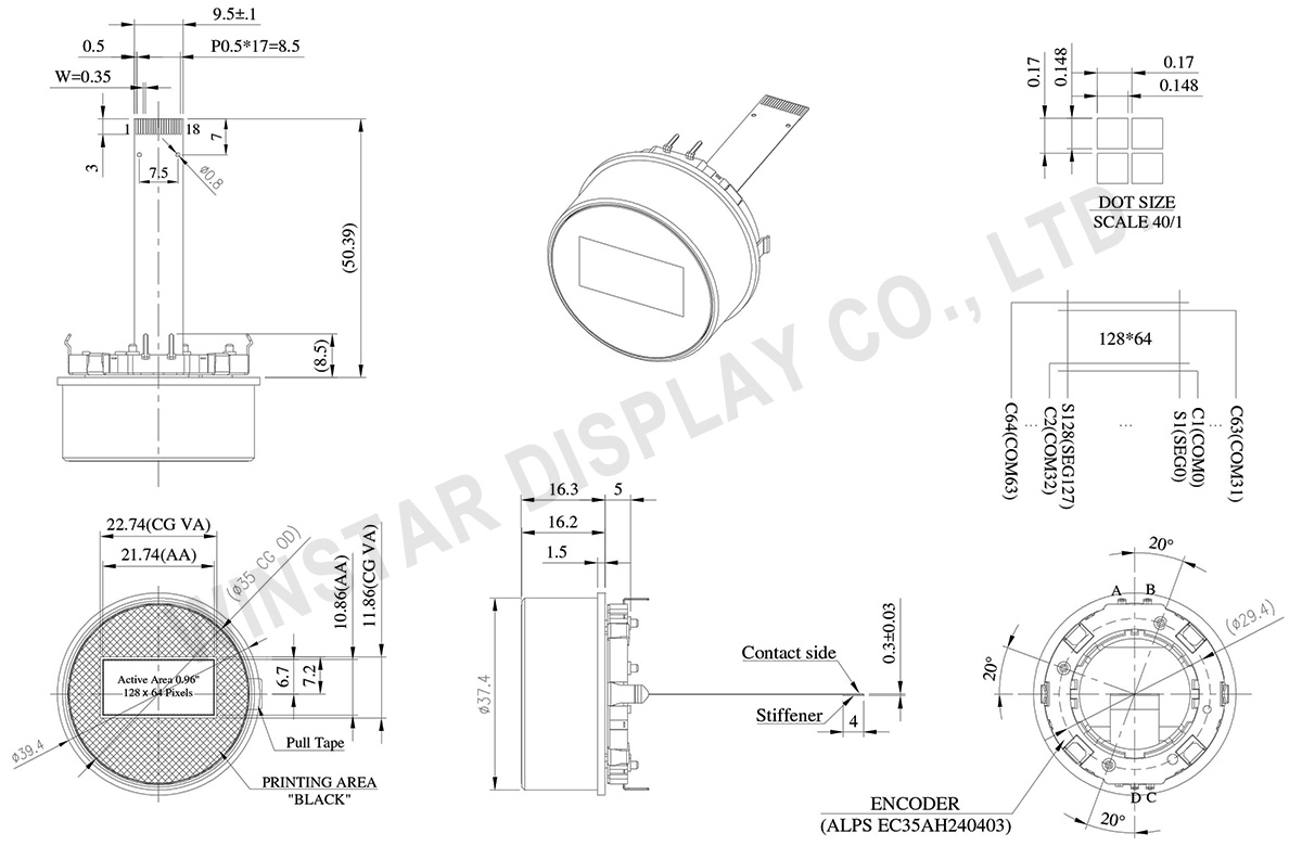
型號 WEO012864Z
►圓形OLED
►類型: 繪圖型
►結構: COG
►尺寸: 0.96吋
►128x64 點陣
►IC:SSD1306
►3V電源電壓
►1/64 duty
►介面: SPI, I2C
►發光顏色: 白色 / 黃色 / 天空藍
WEO012864Z OLED型號是WEO012864D的延伸產品, 此款產品為OLED模組搭配飛梭旋鈕機構設計而成的控制旋鈕,客戶可以直接用於產品應用。此OLED模組為0.96吋COG結購OLED顯示器,解析度由128x64 dots組成,內建SSD1306 IC, 可支援4線SPI和I2C介面。此款模組VCI電源電壓最低1.65V最高3.3V,驅動方式1/64 duty。
WEO012864Z OLED飛梭旋鈕模組,非常適合用於需要控制旋鈕的產品應用,例如:智能居家應用,智能控制設備,影音系統等。模組工作溫度-20℃~+70℃; 儲存溫度-30℃至+80℃。
Data source ref: WEO012864ZLPP3N00000
| 項目 | 尺寸 | 單位 |
|---|---|---|
| 點陣(解析度) | 128 x 64 | Dots |
| 模組尺寸 | Ø39.4 x 24.8 | mm |
| 檢視區域 | 21.74 x 10.86 | mm |
| 點大小 | 0.148 x 0.148 | mm |
| 點間距 | 0.17 x 0.17 | mm |
| 顯示模式 | 被動矩陣 | |
| 發光顏色 | 單色 | |
| 驅動方式 | 1/64 | |
| IC | SSD1326 | |
| 介面 | 4線SPI , I2C | |
| 尺寸 | 0.96吋 | |
| 項目 | 符號 | 最小值 | 最大值 | 單位 |
|---|---|---|---|---|
| 電源電壓 | VCI | -0.3 | 4.0 | V |
| 顯示電源電壓 | VCC | 0 | 15 | V |
| 工作溫度 | TOP | -20 | +70 | °C |
| 儲存溫度 | TST | -30 | +80 | °C |
| 項目 | 符號 | 條件 | 最小值 | 典型值 | 最大值 | 單位 |
|---|---|---|---|---|---|---|
| 電源電壓 | VCI | - | 1.65 | 3.0 | 3.3 | V |
| 顯示電源電壓 | VCC | - | 6 | 10 | 10.5 | V |
| 輸入高準位 | VIH | - | 0.8xVCI | - | - | V |
| 輸入低準位 | VIL | - | - | - | 0.2xVCI | V |
| 輸出高準位 | VOH | Iout = 100uA | 0.9xVCI | - | - | V |
| 輸出低準位 | VOL | Iout = 100uA | - | - | 0.1xVCI | V |
| VCC的工作電流(VCC由外部提供) | ICC | VCC =10V | - | 5 | 10 | mA |
| Pin No. | 符號 | 功能說明 | ||||||
|---|---|---|---|---|---|---|---|---|
| 1 | VSS | Ground pin. | ||||||
| 2 | VCC | Power supply for panel driving voltage. This is also the most positive power voltage supply pin. | ||||||
| 3 | VCOMH | COM signal deselected voltage level. A capacitor should be connected between this pin and VSS. |
||||||
| 4 | VCI | Power supply pin for core logic operation | ||||||
| 5 | NC | No connection | ||||||
| 6 | BS1 | MCU bus interface selection pins. Select appropriate logic setting as described in the following table.
(1) 0 is connected to VSS (2) 1 is connected to VCI |
||||||
| 7 | IREF | This is segment output current reference pin. When external IREF is used, a resistor should be connected between this pin and VSS to maintain the IREF current at a maximum of 30uA. |
||||||
| 8 | CS# | This pin is the chip select input. (active LOW). | ||||||
| 9 | RES# | This pin is reset signal input. When the pin is pulled LOW, initialization of the chip is executed. Keep this pin HIGH during normal operation. |
||||||
| 10 | D/C# | When 4-wire serial interface is selected, this pin is Data/Command control pin connecting to the MCU. In I2C mode, this pin acts as SA0 for slave address selection. |
||||||
| 11 | D0 | These pins are bi-directional data bus connecting to the MCU data bus. When serial interface mode is selected, D0 will be the serial clock input: SCLK; D1 will be the serial data input: SDIN and D2 should be kept NC. When I2C mode is selected, D2, D1 should be tied together and serve as SDAout, SDAin in application and D0 is the serial clock input, SCL. |
||||||
| 12 | D1 | |||||||
| 13 | D2 | |||||||
| 14 | NC | No connection | ||||||
| 15 | NC | No connection | ||||||
| 16 | NC | No connection | ||||||
| 17 | VCC | Power supply for panel driving voltage. This is also the most positive power voltage supply pin. | ||||||
| 18 | VSS | Ground pin. |
| No. | 符號 | 功能說明 |
|---|---|---|
| 1 | FSW_A | Encoder terminal signal-A |
| 2 | FSW_B | Encoder terminal signal-B |
| 3 | FSW_C | Encoder terminal signal-C |
| 4 | FSW_D | Ground |

通過點擊「允許所有 Cookie」,代表您同意在您的設備上存儲 Cookie 以增強網站瀏覽體驗、分析網站使用情況並協助我們的行銷和網站效能優化工作。您可以在我們的隱私權政策中找到有關於此的更多資訊。