
私たちはあなたのプライバシーを大切にします
「すべてのクッキーを許可」をクリックすると、サイトのナビゲーションを向上させ、サイト使用状況を分析し、マーケティングおよびパフォーマンスの取り組みを支援するために、クッキーをデバイスに保存することに同意したことになります。この件に関する詳細情報は、ポリシーをご覧ください。プライバシーポリシー

 - WEO012864J-CTP")
 - WEO012864J-CTP")
 - WEO012864J-CTP")
 - WEO012864J-CTP")
 - WEO012864J-CTP")
 - WEO012864J-CTP")
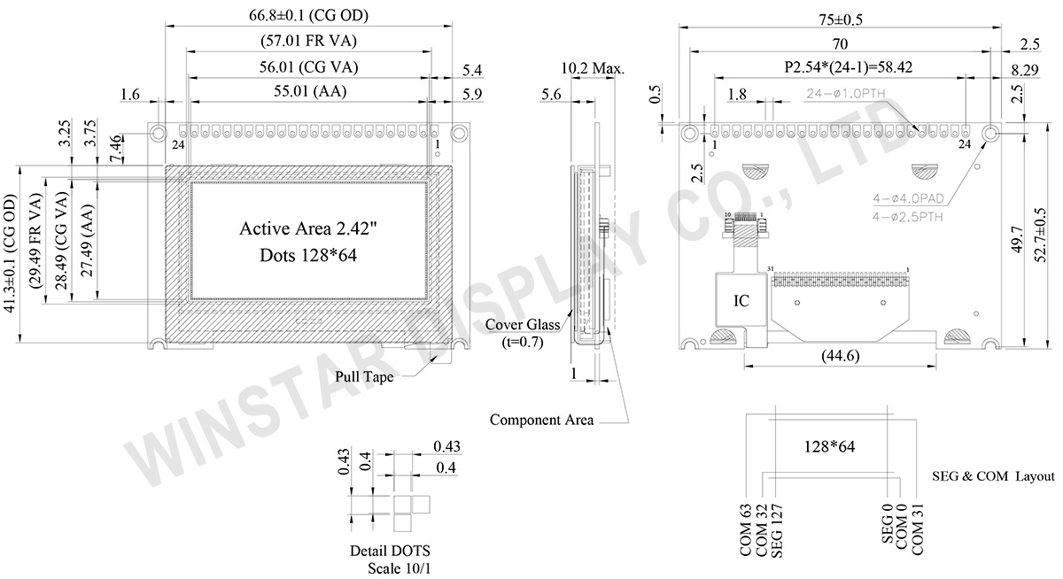
型番 WEO012864J-CTP
►タイプ: グラフィック液晶ELモジュール
►結構: COG+FR+PCB
►サイズ: 2.42インチ
►128 x 64 ドットマトリックス
►IC:SSD1309
►3V電源電圧
►1/64 duty
►インターフェース: プリセット6800・オプション8080, SPI或いはI2C
►静電容量式タッチパネル(CTP)
►検出ポイント: 1
►発光色: 白色 / 黄色 / 空色 / 緑色
WEO012864J-CTP は2.42インチのグラフィック有機ELディスプレイで、静電容量式のタッチパネルを搭載しております。解像度は 128x64 です。 SSD1309 ICを内蔵し、初期設定は 6800 8ビット パラレルインターフェースにしておきます。 8080 パラレルと4線の SPI /I2C のインターフェースを選択可能です。ロジック電源電圧 は3Vで、デューティは 1/64 です。 WEO012864J-CTP モジュールにGT911タッチパネルICを内蔵し、I2Cインターフェースをサポートしており、静電容量方式タッチパネル(CTP)用の検出ポイントを内蔵しております。
このモジュールにはPCBボードが搭載されており、お客様は追加のPCBを開発する必要はありません。さらに、モジュールには4つのネジ穴がある金属フレームが付いており、お客様が簡単に取り付けることができます。この2.42インチの静電容量方式タッチパネル付き WEO012864J機種はスマートホームアプリケーション、 インテリジェントテクノロジーデバイス、 エネルギーシステム、メーターデバイス、通信システム、医療機器などに適しております。 操作温度範囲は -20℃ ~ +70℃で、保存温度範囲は -30℃ ~ +80℃です。
| 項目 | 仕様 | 単位 |
|---|---|---|
| ドットマトリックス(解像度) | 128 x 64 | - |
| 外形寸法 | 75.0 × 52.7 ×10.2 MAX | mm |
| 有効エリア | 55.01 × 27.49 | mm |
| ドットサイズ | 0.40 × 0.40 | mm |
| ドットピッチ | 0.43 × 0.43 | mm |
| 表示モード | パッシブマトリクス | |
| 発光色 | モノクロ | |
| 駆動方法 | 1/64 Duty | |
| IC | SSD1309 | |
| インターフェイス | 8Bits 6800 , オプション 8080 / 4-SPI / I2C | |
| サイズ | 2.42 インチ | |
| PCAP IC | GT911 | |
| 検出ポイント | 1 | |
| PCAP インターフェイス | I2C | |
| 表面処理 | グレア | |
| パラメーター | 記号 | 最小値 | 最大値 | 単位 |
|---|---|---|---|---|
| ロジック電源電圧 | VDD | -0.3 | 4 | V |
| 操作温度 | TOP | -20 | +70 | °C |
| 保存温度 | TSTG | -30 | +80 | °C |
| 項目 | 記号 | 条件 | 最小値 | 典型値 | 最大値 | 単位 |
|---|---|---|---|---|---|---|
| ロジック電源電圧 | VDD | - | 2.8 | 3.0 | 3.3 | V |
| 高レベル入力 | VIH | - | 0.8×VDD | - | - | V |
| 低レベル入力 | VIL | - | - | - | 0.2×VDD | V |
| 高レベル出力 | VOH | - | 0.9×VDD | - | - | V |
| 低レベル出力 | VOL | - | - | - | 0.1×VDD | V |
| 50% Check Board operating Current | IDD | VDD =3V | - | 150 | 300 | mA |
| No. | 記号 | ピン功能定義 |
|---|---|---|
| 1 | VDD | Power supply pin for core logic operation |
| 2 | VSS | Ground. |
| 3 | NC(GND) | No connection |
| 4~11 | D0~D7 | These pins are bi-directional data bus connecting to the MCU data bus. Unused pins are recommended to tie LOW. |
| 12 | CS# | This pin is the chip select input connecting to the MCU. The chip is enabled for MCU communication only when CS# is pulled LOW (active LOW). |
| 13 | NC(GND) | No connection |
| 14 | RES# | This pin is reset signal input. When the pin is pulled LOW, initialization of the chip is executed. Keep this pin pull HIGH during normal operation. |
| 15 | R/W# | This pin is read / write control input pin connecting to the MCU interface. When 6800 interface mode is selected, this pin will be used as Read/Write (R/W#) selection input. Read mode will be carried out when this pin is pulled HIGH and write mode when LOW. |
| 16 | D/C# | This pin is Data/Command control pin connecting to the MCU. When the pin is pulled HIGH, the data at D[7:0] will be interpreted as data. When the pin is pulled LOW, the data at D[7:0] will be transferred to a command register. |
| 17 | E | This pin is MCU interface input. When 6800 interface mode is selected, this pin will be used as the Enable (E) signal. |
| 18 | NC(GND) | No connection |
| 19 | DISP | No Connection |
| 20 | NC(GND) | No connection |
| 21 | TP_INT | Interrupt signal, active low, asserted to request Host start a new transaction |
| 22 | TP_SDA | I2C data signal |
| 23 | TP_SCL | I2C clock signal |
| 24 | TP_RST | External reset signal, active low |

「すべてのクッキーを許可」をクリックすると、サイトのナビゲーションを向上させ、サイト使用状況を分析し、マーケティングおよびパフォーマンスの取り組みを支援するために、クッキーをデバイスに保存することに同意したことになります。この件に関する詳細情報は、ポリシーをご覧ください。プライバシーポリシー