

私たちはあなたのプライバシーを大切にします
「すべてのクッキーを許可」をクリックすると、サイトのナビゲーションを向上させ、サイト使用状況を分析し、マーケティングおよびパフォーマンスの取り組みを支援するために、クッキーをデバイスに保存することに同意したことになります。この件に関する詳細情報は、ポリシーをご覧ください。プライバシーポリシー

、2.26インチ- WEO001602C")
、2.26インチ- WEO001602C")
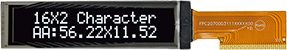
16x2行 COG 字符 OLED ディスプレイモジュール(型番:WEO001602C)は、COG(Chip On Glass)設計を採用しており、高性能で信頼性の高いディスプレイソリューションを提供します。この OLED モジュールは、優れた表示品質と耐久性で広く利用されています。
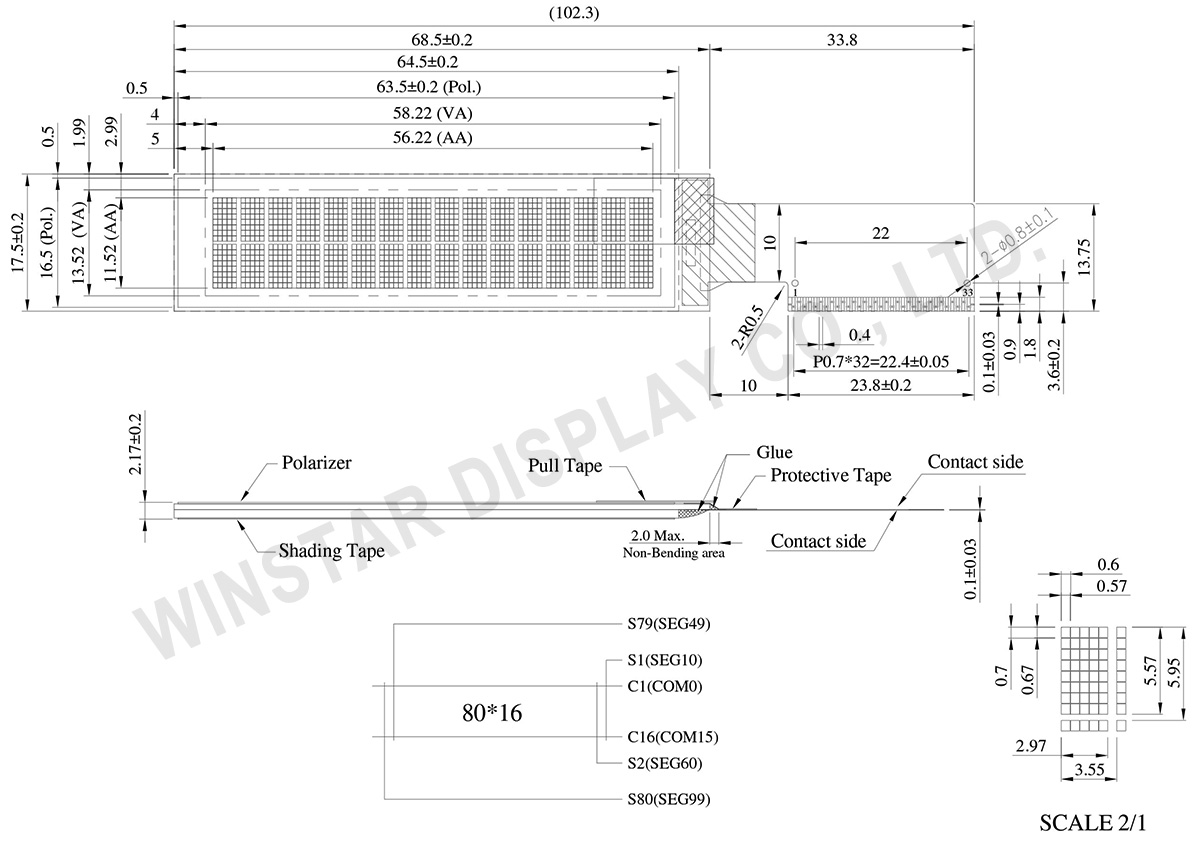
このモジュールの寸法は 68.5 x 17.5 mm で、厚さは 2.17 mm です。表示エリアの有効寸法は 56.22 x 11.52 mm で、対角線のサイズは 2.26 インチです。SSD1311 ドライバー IC を搭載しており、ASCII、英語、欧文、日文など、さまざまな文字セットを表示できます。各文字は 5x8 ピクセルで構成されており、詳細で明瞭な表示が可能です。
このモジュールの表示モードは 2 行で、各行に 16 文字を表示できます。OLED 技術の自発光特性により、バックライトが不要で、より軽量で薄型のデザインを実現しています。また、コントラスト比は 10,000:1 に達し、超広視野角(最大 175 度)を備えており、異なる角度から見ても一貫した表示品質を保ちます。さらに、低消費電力と広い動作温度範囲を持ち、優れた適応性を示しています。
WEO001602C の動作温度範囲は -40°C から +80°C で、保存温度範囲は -40°C から +85°C です。極端な環境でも安定して動作します。モジュールのロジック電圧範囲は 2.4V から 3.3V で、典型値は 3V です。また、1/16 duty ドライビング方式を採用しています。
さらに、WEO001602Cは6800/8080 8ビット並列インターフェースおよびI2C/SPIシリアルインターフェースなど、複数のインターフェースオプションをサポートしており、さまざまなシステム要件に対応する柔軟な接続が可能です。モジュールシリーズは、多様な顧客ニーズに応えるためのさまざまなフレキシブルプリント回路(FPC)オプションも提供しています。
その卓越した表示品質、広範な動作温度範囲、柔軟なインターフェースオプションにより、WEO001602C OLED ディスプレイモジュールは、従来の LCD モジュールの理想的な代替品となります。この 16x2 字符 OLED モジュールを使用することで、製品の表示性能を向上させ、より高い表示品質と低い消費電力を実現することをお勧めします。
 FPC Options
| 項目 | サイズ | 単位 |
|---|---|---|
| 表示形式 | 16文字x2行 | - |
| モジュールサイズ | 68.5 x 17.5 x 2.17 | mm |
| 表示エリア | 58.22 x 13.52 | mm |
| アクティブエリア | 56.22 x 11.52 | mm |
| ドットサイズ | 0.57 x 0.67 | mm |
| ドットピッチ | 0.60 x 0.70 | mm |
| 文字サイズ | 2.97 x 5.57 | mm |
| 文字ピッチ | 3.55 x 5.95 | mm |
| パネルタイプ | OLED , モノクロ | |
| Duty | 1/16 | |
| IC | SSD1311 | |
| インターフェイス | 6800, 8080, SPI, I2C | |
| 表示サイズ | 2.26 インチ | |
| 項目 | 記号 | 最小値 | 最大値 | 単位 |
|---|---|---|---|---|
| ロジック電源電圧 | VDD | -0.3 | VDDIO | V |
| 入力/出力ピンの電源電圧 | VDDIO | -0.3 | 6 | V |
| 操作電圧 | VCC | 0 | 16 | V |
| 操作温度 | TOP | -40 | +80 | ℃ |
| 保存温度 | TST | -40 | +85 | ℃ |
| 項目 | 記号 | 条件 | 最小値 | 典型値 | 最大値 | 単位 |
|---|---|---|---|---|---|---|
| ロジック電源電圧 | VDD | Low Voltage I/O | 2.4 | 3.0 | 3.3 | V |
| 5V I/O (VDD as output) |
- | - | - | V | ||
| 入力/出力ピンの電源電圧 | VDDIO | Low Voltage I/O | 2.4 | 3.0 | 3.3 | V |
| 5V I/O | 4.4 | 5.0 | 5.3 | V | ||
| OLED電源電圧 | VCC | - | 8.0 | 10.0 | 10.5 | V |
| - | 8.0 | 12.0 | 12.5 | V | ||
| 高レベル入力電圧 | VIH | - | 0.8xVDDIO | - | - | V |
| 低レベル入力電圧 | VIL | - | - | - | 0.2xVDDIO | V |
| 高レベル出力電圧 | VOH | IOH=-0.5mA | 0.9xVDDIO | - | - | V |
| 低レベル出力電圧 | VOL | IOL=0.5mA | - | - | 0.1xVDDIO | V |
| 50% Check Board Operating Current | ICC | VCC=10V | - | 16 | 24 | mA |
| VCC=12V | - | 18 | 27 | mA |
| Pin No. | 記号 | Pin タイプ | 説明 | ||||||||||||||||||||
|---|---|---|---|---|---|---|---|---|---|---|---|---|---|---|---|---|---|---|---|---|---|---|---|
| 1 | NC | - | No connection | ||||||||||||||||||||
| 2 | VSL | P | This is segment voltage (output low level) reference pin. When external VSL is not used, this pin should be left open. When external VSL is used, connect with resistor and diode to ground (details depend on application). |
||||||||||||||||||||
| 3 | VSS | P | Ground pin. It must be connected to external ground. | ||||||||||||||||||||
| 4 | REGVDD | I | Internal VDD regulator selection pin in 5V I/O application mode. When this pin is pulled HIGH, internal VDD regulator is enabled (5V I/O application). When this pin is pulled LOW, internal VDD regulator is disabled (Low voltage I/O application). |
||||||||||||||||||||
| 5 | SHLC | I | This pin is used to determine the Common output scanning direction. COM scan direction
(1) 0 is connected to VSS (2) 1 is connected to VDDIO |
||||||||||||||||||||
| 6 | SHLS | I | This pin is used to change the mapping between the display data column address and the Segment driver. SEG scan direction
(1) 0 is connected to VSS (2) 1 is connected to VDDIO |
||||||||||||||||||||
| 7 | VDD | P | Power supply for core logic operation. VDD can be supplied externally or regulated internally. In LV IO application (internal VDD is disabled), this is a power input pin. In 5V IO application (internal VDD is enabled), VDD is regulated internally from VDDIO. A capacitor should be connected between VDD and VSS under all circumstances. |
||||||||||||||||||||
| 8 | VDDIO | P | Low voltage power supply and power supply for interface logic level in both Low Voltage I/O and 5V I/O application. It should match with the MCU interface voltage level and must be connected to external source. | ||||||||||||||||||||
| 9 | BS0 | I | MCU bus interface selection pins. Select appropriate logic setting as described in the following table. BS2, BS1 and BS0 are pin select. Bus Interface selection
Note (1) 0 is connected to VSS (2) 1 is connected to VDDIO |
||||||||||||||||||||
| 10 | BS1 | ||||||||||||||||||||||
| 11 | BS2 | ||||||||||||||||||||||
| 12 | GPIO | I/O | It is a GPIO pin. Details refer to OLED command DCh. | ||||||||||||||||||||
| 13 | CS# | I | This pin is the chip select input connecting to the MCU. The chip is enabled for MCU communication only when CS# is pulled LOW (active LOW). In I2C mode, this pin must be connected to VSS. |
||||||||||||||||||||
| 14 | RES# | I | This pin is reset signal input. When the pin is pulled LOW, initialization of the chip is executed. Keep this pin pull HIGH during normal operation. |
||||||||||||||||||||
| 15 | D/C# | I | This pin is Data/Command control pin connecting to the MCU. When the pin is pulled HIGH, the data at D[7:0] will be interpreted as data. When the pin is pulled LOW, the data at D[7:0] will be transferred to a command register. In I2C mode, this pin acts as SA0 for slave address selection. When serial interface is selected, this pin must be connected to VSS. |
||||||||||||||||||||
| 16 | R/W#(WR#) | I | This pin is read / write control input pin connecting to the MCU interface. When 6800 interface mode is selected, this pin will be used as Read/Write (R/W#) selection input. Read mode will be carried out when this pin is pulled HIGH and write mode when LOW. When 8080 interface mode is selected, this pin will be the Write (WR#) input. Data write operation is initiated when this pin is pulled LOW and the chip is selected. When serial or I2C interface is selected, this pin must be connected to VSS. |
||||||||||||||||||||
| 17 | E(RD#) | I | This pin is MCU interface input. When 6800 interface mode is selected, this pin will be used as the Enable (E) signal. Read/write operation is initiated when this pin is pulled HIGH and the chip is selected. When 8080 interface mode is selected, this pin receives the Read (RD#) signal. Read operation is initiated when this pin is pulled LOW and the chip is selected. When serial or I2C interface is selected, this pin must be connected to VSS. |
||||||||||||||||||||
| 18 | D0 | I/O | These pins are bi-directional data bus connecting to the MCU data bus. Unused pins are recommended to tie LOW. When serial interface mode is selected, D0 will be the serial clock input: SCLK; D1 will be the serial data input: SID and D2 will be the serial data output: SOD. When I2C mode is selected, D2, D1 should be tied together and serve as SDAout, SDAin in application and D0 is the serial clock input, SCL. |
||||||||||||||||||||
| 19 | D1 | ||||||||||||||||||||||
| 20 | D2 | ||||||||||||||||||||||
| 21 | D3 | ||||||||||||||||||||||
| 22 | D4 | ||||||||||||||||||||||
| 23 | D5 | ||||||||||||||||||||||
| 24 | D6 | ||||||||||||||||||||||
| 25 | D7 | ||||||||||||||||||||||
| 26 | IREF | I | This pin is the segment output current reference pin. IREF is supplied externally. A resistor should be connected between this pin and VSS to maintain current of around 15uA. |
||||||||||||||||||||
| 27 | ROM0 | I | These pins are used to select Character ROM; select appropriate logic setting as described in the following table. ROM1 and ROM0 are pin select as shown in below table: Character ROM selection
(1) 0 is connected to VSS (2) 1 is connected to VDDIO |
||||||||||||||||||||
| 28 | ROM1 | ||||||||||||||||||||||
| 29 | OPR0 | I | This pin is used to select the character number of character generator. Character RAM selection
(1) 0 is connected to VSS (2) 1 is connected to VDDIO |
||||||||||||||||||||
| 30 | OPR1 | ||||||||||||||||||||||
| 31 | VCOMH | P | COM signal deselected voltage level. A capacitor should be connected between this pin and VSS. No external power supply is allowed to connect to this pin. |
||||||||||||||||||||
| 32 | VCC | P | Power supply for panel driving voltage. This is also the most positive power voltage supply pin. It is supplied by external high voltage source. | ||||||||||||||||||||
| 33 | NC | - | No connection |
| Drawing | FPC Length | PIN | Pitch | ZIF FPC or HOTBAR FPC | Interface | FPC No. | Create Date |
|---|---|---|---|---|---|---|---|
 |
35.2 | 31 | 0.7 | HOTBAR FPC | 6800, 8080, SPI, I2C | FPC2070003111XXXXX00 | 20120208 |
 |
31 | 34 | 0.5 | ZIF FPC | 6800, 8080, SPI, I2C | FPC2005003421XXXXX00 | 20161028 |
Search keyword: oled 16x2, 16x2 oled

「すべてのクッキーを許可」をクリックすると、サイトのナビゲーションを向上させ、サイト使用状況を分析し、マーケティングおよびパフォーマンスの取り組みを支援するために、クッキーをデバイスに保存することに同意したことになります。この件に関する詳細情報は、ポリシーをご覧ください。プライバシーポリシー