2.7 inç 128x64 COG OLED Ekran, PCB ve Çerçeve Desteği ile Grayscale
Model No. WEP012864U
►Türü : Grafik
►Yapı : COG + Çerçeve + PCB
►Boyut : 2.7 inç
►128 x 64 dot matrisi
►IC:SSD1357
►3V güç sağlayıcı
►1/64 görev
►Ara yüz : 6800, 8080, SPI, I2C
►OLED Rengi: Beyaz / Sarı
►Gri Tonlama Desteği
Açıklama
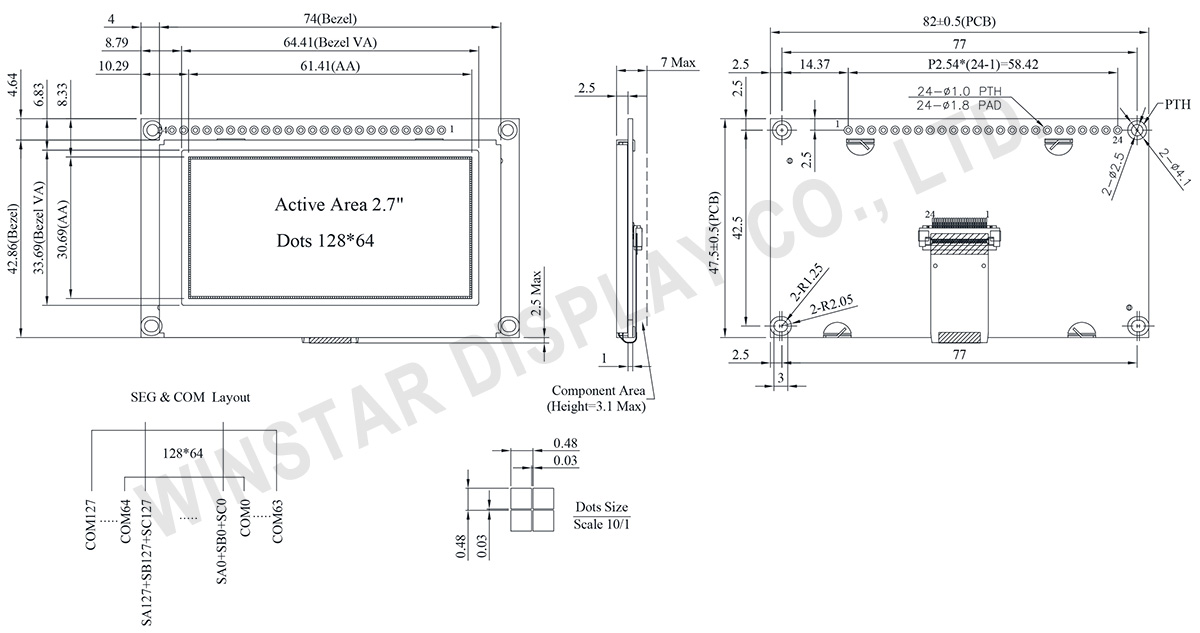
WEP012864U, COG yapıya sahip 128x64 noktalı çözünürlüğe ve 2.7 inç (61.41 × 30.69 mm) aktif alana sahip grafik bir OLED ekran modülüdür. Modül, 6800/8080 8-bit ve 4 tel SPI ile birlikte I2C arabirimlerini destekleyen SSD1357 IC ile donatılmıştır. Ekran, 3V mantık voltajı ve 1/64 görev döngüsü ile 4-bit gri tonlamayı destekler.
WEP012864U OLED serisi, uygulamaya teller aracılığıyla kolayca bağlanabilen bir metal çerçeve ve PCB kart ile birlikte gelir. Müşterilerin ek PCB kartlar geliştirmeleri gerekmez, çünkü arayüz ayarlarını ve VCC devrelerini entegre eder, kullanıcı deneyimini basitleştirir. PCB, modülün uygulama ürününe kolayca monte edilmesi için dört vida deliği ile tasarlanmıştır.
Bu OLED modülü, 10.000:1 yüksek kontrast oranına sahiptir, bu da daha canlı ve derin siyahlar ile daha parlak beyazların mümkün olmasını sağlar. Bu, geliştirilmiş görüntü kalitesi, daha keskin detaylar ve arttırılmış okunabilirlik anlamına gelir. Modül, -40℃ ila 80℃ arasındaki bir sıcaklık aralığında çalışır ve -40℃ ila 85℃ arasındaki depolama sıcaklıklarını kapsar.
Duvar/sayaç cihazları, ev uygulamaları, finans-POS, Bulut/IoT sistemleri, akıllı teknoloji cihazları, enerji sistemleri, iletişim sistemleri, tıbbi cihazlar vb. için idealdir.
Ayrıca, benzer OLED panelleri, metal çerçeve olmadan PCB ve metal çerçeveli ancak PCB olmadan WEO012864U serisinde ve WEF012864U serisinde bulunmaktadır. Dokunmatik işlev gereksinimleriniz varsa, lütfen WEP012864U-CTP serisini düşünün.
ÇIZIM
Data source ref:WEP012864ULAP3N00000
AYRINTILAR
Arayüz Pin Fonksiyonlari
No. | Sembol | Fonksiyon | |||||||||||||||
---|---|---|---|---|---|---|---|---|---|---|---|---|---|---|---|---|---|
1 | VSS | This is a ground pin. | |||||||||||||||
2 | VDD | Power supply pin for core logic operation | |||||||||||||||
3 | NC | Reserved Pin The N.C. pin between function pins is reserved for compatible and flexible design. |
|||||||||||||||
4 | D/C# | This pin is Data/Command control pin connecting to the MCU. When the pin is pulled HIGH, the data at D[7:0] will be interpreted as data. When the pin is pulled LOW, the data at D[7:0] will be transferred to a command register. In I2C mode, this pin acts as SA0 for slave address selection. |
|||||||||||||||
5 | R/W# (WR#) |
This pin is read / write control input pin connecting to the MCU interface. When 6800 interface mode is selected, this pin will be used as Read/Write (R/W#) selection input. Read mode will be carried out when this pin is pulled HIGH and write mode when LOW. When 8080 interface mode is selected, this pin will be the Write (WR#) input. Data write operation is initiated when this pin is pulled LOW and the chip is selected. When serial or I2C interface is selected, this pin must be connected to VSS. |
|||||||||||||||
6 | E/RD# | This pin is MCU interface input. When 6800 interface mode is selected, this pin will be used as the Enable (E) signal. Read/write operation is initiated when this pin is pulled HIGH and the chip is selected. When 8080 interface mode is selected, this pin receives the Read (RD#) signal. Read operation is initiated when this pin is pulled LOW and the chip is selected. When serial or I2C interface is selected, this pin must be connected to VSS. |
|||||||||||||||
7 | DB0 | These pins are bi-directional data bus connecting to the MCU data bus. Unused pins are recommended to tie LOW. When serial interface mode is selected, D0 will be the serial clock input: SCLK; D1 will be the serial data input: SDIN. When I2C mode is selected, D2, D1 should be tied together and serve as SDAout, SDAin in application and D0 is the serial clock input, SCL. |
|||||||||||||||
8 | DB1 | ||||||||||||||||
9 | DB2 | ||||||||||||||||
10 | DB3 | ||||||||||||||||
11 | DB4 | ||||||||||||||||
12 | DB5 | ||||||||||||||||
13 | DB6 | ||||||||||||||||
14 | DB7 | ||||||||||||||||
15 |
NC | No connection. | |||||||||||||||
16 | RES# | This pin is reset signal input. When the pin is pulled LOW, initialization of the chip is executed. Keep this pin pull HIGH during normal operation. |
|||||||||||||||
17 |
CS# | Chip Select This pin is the chip select input. The chip is enabled for MCU communication only when CS# is pulled low. |
|||||||||||||||
18 | NC | No connection. | |||||||||||||||
19 | BS2 | Communicating Protocol Select. These pins are MCU interface selection input. See the following table:
|
|||||||||||||||
20 | BS1 | ||||||||||||||||
21 | NC | No connection. | |||||||||||||||
22 | NC | No connection. | |||||||||||||||
23 | NC | No connection. | |||||||||||||||
24 | NC | No connection. |
Mekanik Veri
Kalem | Ölçü | Birim |
---|---|---|
Nokta Matrisi | 128 x 64 | Dots |
Modül ölçüleri | 82.0 × 47.5 × 7 Max. | mm |
Aktif alan | 61.41 × 30.69 | mm |
Nokta boyutu | 0.45 × 0.45 | mm |
Nokta sıklığı | 0.48 × 0.48 | mm |
Display Mode | Pasif Matrisli | |
Display Color | Monokrom | |
Drive Duty | 1/64 Duty | |
Gray Scale | 4 bits | |
IC | SSD1357 | |
Arayüz | 6800, 8080, SPI, I2C | |
Boyut | 2.7 inç |
Maksimum Değerler
Parameter | Sembol | Minumum Deger | Maksimum Deger | Birim |
---|---|---|---|---|
Supply Voltage for Logic | VDD | -0.3 | 4.0 | V |
Çalışma Sıcaklığı | TOP | -40 | 80 | °C |
Saklama Sıcaklığı | TSTG | -40 | 85 | °C |
Elektronik Özellikleri
Kalem | Sembol | Durum | Minumum Deger | Tipik Deger | Maksimum Deger | Birim |
---|---|---|---|---|---|---|
Supply Voltage for Logic | VDD | - | 2.8 | 3.0 | 3.3 | V |
High Level Input | VIH | - | 0.8×VDD | - | - | V |
Low Level Input | VIL | - | - | - | 0.2×VDD | V |
High Level Output | VOH | - | 0.9×VDD | - | - | V |
Low Level Output | VOL | - | - | - | 0.1×VDD | V |
Display 50% Pixel on | IDD | VDD =3V | - | 120 | 180 | mA |