Display OLED COG da 2,7 pollici, 128x64, supporto scala di grigi con PCB e telaio
Modello numero WEP012864U
►Tipo: grafico
►Struttura: COG + cornice + PCB
►Dimensione: 2.7 pollici
►128 x 64 a matrice di punti
►IC:SSD1357
►Alimentatore 3V
►1/64 duty
►Interfaccia: 6800, 8080, SPI, I2C
►Colore display: Bianco / Giallo
►Support Grayscale
Descrizione
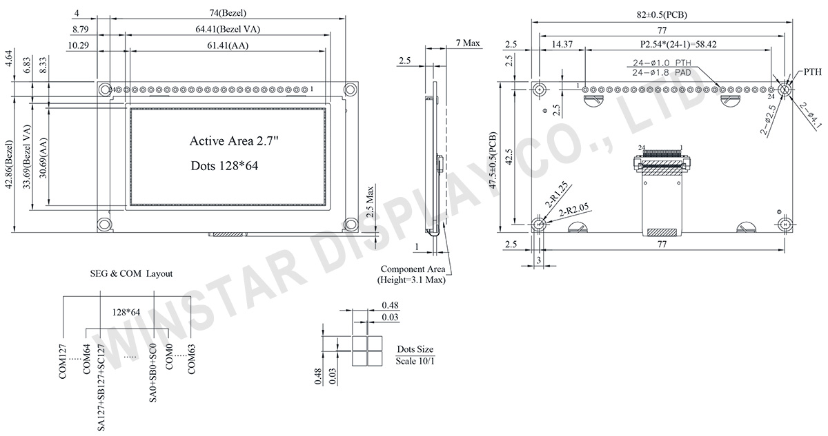
Il WEP012864U è un display OLED grafico con struttura COG, risoluzione di 128x64 pixel e un'area attiva di 2,7 pollici (61,41 × 30,69 mm). Il modulo è dotato del controller SSD1357, supporta le interfacce 6800/8080 a 8 bit e SPI a 4 fili, oltre alle interfacce I2C. Il display supporta la scala di grigi a 4 bit, con una tensione logica di 3V e un ciclo di lavoro di 1/64.
La serie OLED WEP012864U è fornita con una cornice metallica e una scheda PCB che si connette facilmente all'applicazione tramite cavi. Ai clienti non è richiesto lo sviluppo di ulteriori schede PCB, in quanto integra le impostazioni dell'interfaccia e i circuiti VCC, semplificando l'esperienza dell'utente. La PCB è progettata con quattro fori filettati per facilitare l'installazione del modulo sul prodotto dell'applicazione.
Questo modulo OLED vanta un elevato rapporto di contrasto di 10.000:1, consentendo neri più vibranti e profondi, così come bianchi più luminosi. Ciò porta a un miglioramento della qualità dell'immagine, dettagli più nitidi e una migliore leggibilità. Il modulo è operativo in un intervallo di temperatura da -40℃ a 80℃, con temperature di conservazione che vanno da -40℃ a 85℃.
È ideale per dispositivi da parete/contatori, applicazioni domestiche, sistemi finanziari-POS, sistemi Cloud/IoT, dispositivi tecnologici intelligenti, sistemi energetici, sistemi di comunicazione, strumenti medici, ecc.
Inoltre, pannelli OLED simili sono disponibili nella serie WEO012864U senza cornice metallica e PCB e nella serie WEF012864U con cornice metallica ma senza PCB. Se hai requisiti per la funzionalità touch, considera la serie WEP012864U-CTP.
DISEGNO
Data source ref:WEP012864ULAP3N00000
SPECIFICHE TECNICHE
Funzione dei Pin di Interfaccia
No. | Simbolo | Funzione | |||||||||||||||
---|---|---|---|---|---|---|---|---|---|---|---|---|---|---|---|---|---|
1 | VSS | This is a ground pin. | |||||||||||||||
2 | VDD | Power supply pin for core logic operation | |||||||||||||||
3 | NC | Reserved Pin The N.C. pin between function pins is reserved for compatible and flexible design. |
|||||||||||||||
4 | D/C# | This pin is Data/Command control pin connecting to the MCU. When the pin is pulled HIGH, the data at D[7:0] will be interpreted as data. When the pin is pulled LOW, the data at D[7:0] will be transferred to a command register. In I2C mode, this pin acts as SA0 for slave address selection. |
|||||||||||||||
5 | R/W# (WR#) |
This pin is read / write control input pin connecting to the MCU interface. When 6800 interface mode is selected, this pin will be used as Read/Write (R/W#) selection input. Read mode will be carried out when this pin is pulled HIGH and write mode when LOW. When 8080 interface mode is selected, this pin will be the Write (WR#) input. Data write operation is initiated when this pin is pulled LOW and the chip is selected. When serial or I2C interface is selected, this pin must be connected to VSS. |
|||||||||||||||
6 | E/RD# | This pin is MCU interface input. When 6800 interface mode is selected, this pin will be used as the Enable (E) signal. Read/write operation is initiated when this pin is pulled HIGH and the chip is selected. When 8080 interface mode is selected, this pin receives the Read (RD#) signal. Read operation is initiated when this pin is pulled LOW and the chip is selected. When serial or I2C interface is selected, this pin must be connected to VSS. |
|||||||||||||||
7 | DB0 | These pins are bi-directional data bus connecting to the MCU data bus. Unused pins are recommended to tie LOW. When serial interface mode is selected, D0 will be the serial clock input: SCLK; D1 will be the serial data input: SDIN. When I2C mode is selected, D2, D1 should be tied together and serve as SDAout, SDAin in application and D0 is the serial clock input, SCL. |
|||||||||||||||
8 | DB1 | ||||||||||||||||
9 | DB2 | ||||||||||||||||
10 | DB3 | ||||||||||||||||
11 | DB4 | ||||||||||||||||
12 | DB5 | ||||||||||||||||
13 | DB6 | ||||||||||||||||
14 | DB7 | ||||||||||||||||
15 |
NC | No connection. | |||||||||||||||
16 | RES# | This pin is reset signal input. When the pin is pulled LOW, initialization of the chip is executed. Keep this pin pull HIGH during normal operation. |
|||||||||||||||
17 |
CS# | Chip Select This pin is the chip select input. The chip is enabled for MCU communication only when CS# is pulled low. |
|||||||||||||||
18 | NC | No connection. | |||||||||||||||
19 | BS2 | Communicating Protocol Select. These pins are MCU interface selection input. See the following table:
|
|||||||||||||||
20 | BS1 | ||||||||||||||||
21 | NC | No connection. | |||||||||||||||
22 | NC | No connection. | |||||||||||||||
23 | NC | No connection. | |||||||||||||||
24 | NC | No connection. |
Dati meccanici
Articolo | Dimensioni | Unità |
---|---|---|
A matrice di punti | 128 x 64 | punti |
Dimensione del modulo | 82.0 × 47.5 × 7 Max. | mm |
Area attiva | 61.41 × 30.69 | mm |
Dimensioni del Dot | 0.45 × 0.45 | mm |
Passo del Dot | 0.48 × 0.48 | mm |
Modalità display | Matrice passiva | |
Colore display | monocromatici | |
Drive Duty | 1/64 Duty | |
Gray Scale | 4 bits | |
IC | SSD1357 | |
Interfaccia | 6800, 8080, SPI, I2C | |
Dimensione | 2.7 pollici |
Valori massimi assoluti
Parameter | Simbolo | Valore Min | Valore massimo | Unità |
---|---|---|---|---|
Supply Voltage for Logic | VDD | -0.3 | 4.0 | V |
Temperatura di lavoro | TOP | -40 | 80 | °C |
Temperatura di stock | TSTG | -40 | 85 | °C |
Caratteristiche elettriche
Articolo | Simbolo | Condizione | Valore Min | Valore tipico | Valore massimo | Unità |
---|---|---|---|---|---|---|
Supply Voltage for Logic | VDD | - | 2.8 | 3.0 | 3.3 | V |
High Level Input | VIH | - | 0.8×VDD | - | - | V |
Low Level Input | VIL | - | - | - | 0.2×VDD | V |
High Level Output | VOH | - | 0.9×VDD | - | - | V |
Low Level Output | VOL | - | - | - | 0.1×VDD | V |
Display 50% Pixel on | IDD | VDD =3V | - | 120 | 180 | mA |