
 - WEX025664B")
 - WEN025664B")
我们重视您的隐私
通过点击「允许所有 Cookie」,代表您同意在您的设备上存储 Cookie 以增强网站浏览体验、分析网站使用情况并协助我们的营销和网站效能优化工作。您可以在我们的隐私权政策中找到有关于此的更多信息。
 - WEX025664B-CTP")
 - WEX025664B-CTP")
 - WEX025664B-CTP")
 - WEX025664B-CTP")
 - WEX025664B-CTP")
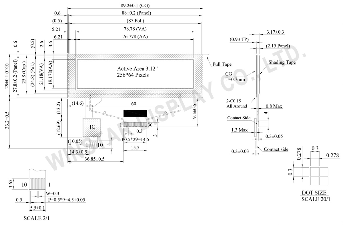
WEX025664B-CTP是一款3.12英寸 COF 结构单色图形 OLED 显示模块,集成电容式触控面板(CTP),分辨率为256×64 dots。该模块采用SSD1322驱动IC,支持6800/8080 8-bit 并行接口以及3/4 线 SPI 接口。模块外形尺寸为89.2 × 29.0 mm,显示区域为76.778 × 19.178 mm。
该OLED模块支持4-bit 灰度显示,工作电压为3.0V(typ.),采用1/64 duty 驱动方式。工作温度范围为-20°C 至 +70°C,存储温度范围为-30°C 至 +80°C。内建触控面板采用FT6336U控制器,支持I²C 接口及单点触控。
WEX025664B-CTP适用于壁挂式设备、POS系统、IoT设备、手持仪器、通信设备及医疗设备等应用,同时也适用于从传统STN显示升级至OLED的应用场景。
同系列OLED面板还提供以下不同结构选项:
| 项目 | 尺寸 | 单位 |
|---|---|---|
| 点阵 | 256 x 64 Dots | - |
| 模块尺寸 | 89.2 × 29.0 × 3.17 | mm |
| 有效区域 | 76.778×19.178 | mm |
| 点大小 | 0.278×0.278 | mm |
| 点间距 | 0.3×0.3 | mm |
| 显示模式 | 被动矩阵 | |
| 发光颜色 | 单色 | |
| 驱动方式 | 1/64 Duty | |
| 灰阶 | 4 bits | |
| OLED IC | SSD1322 (COF) | |
| OLED 接口 | 6800, 8080, SPI | |
| 尺寸(对角线) | 3.12 寸 | |
| CTP IC | FT6336U | |
| 支援手指数 | 1 | |
| CTP 接口 | I2C | |
| 表面 | 亮面 | |
| 参数 | 符号 | 最小值 | 最大值 | 单位 |
|---|---|---|---|---|
| 工作电源电压 | VCI | -0.3 | 4 | V |
| 逻辑电源电压 | VDD | -0.5 | 2.75 | V |
| I/O pin 供电电压 | VDDIO | -0.5 | VCI | V |
| 显示电源电压 | VCC | -0.5 | 20 | V |
| 工作温度 | TOP | -20 | +70 | °C |
| 储存温度 | TSTG | -30 | +80 | °C |
| 参数 | 符号 | 最小值 | 最大值 | 单位 |
|---|---|---|---|---|
| 电源电压 | VDD | -0.3 | 3.6 | V |
| 项目 | 符号 | 条件 | 最小值 | 典型值 | 最大值 | 单位 |
|---|---|---|---|---|---|---|
| 工作电源电压 | VCI | Note | 2.8 | 3.0 | 3.3 | V |
| 显示电源电压 | VCC | - | 14 | 14.5 | 15 | V |
| 逻辑电源电压 | VDD | - | 2.4 | - | 2.6 | V |
| I/O Pin 电源 | VDDIO | - | 1.65 | VCI | V | |
| 输入高准位 | VIH | - | 0.8×VDDIO | - | VDDIO | V |
| 输入低准位 | VIL | - | 0 | - | 0.2×VDDIO | V |
| 输出高准位 | VOH | - | 0.9×VDDIO | - | VDDIO | V |
| 输出低准位 | VOL | - | 0 | - | 0.1×VDDIO | V |
| 50%显示画面耗电流 | VCC =14.5V | - | 32 | 48 | mA | |
| 项目 | 符号 | 条件 | 最小值 | 典型值 | 最大值 | 单位 |
|---|---|---|---|---|---|---|
| 电源电压 | VDD | 2.8 | 3.0 | 3.3 | V | |
| 输入高准位 | VIH | 0.7xVDD | - | VDD | V | |
| 输入低准位 | VIL | -0.3 | - | 0.3xVDD | V | |
| 输出高准位 | VOH | IOH = -0.1mA | 0.7xVDD | - | - | V |
| 输出低准位 | VOL | IOH = 0.1mA | - | - | 0.3xVDD | V |
| No. | 符号 | 功能说明 | ||||||||||
|---|---|---|---|---|---|---|---|---|---|---|---|---|
| 1 | N.C. | Reserved Pin The N.C. pin between function pins are reserved for compatible and flexible design. |
||||||||||
| 2 | VSS | Ground. | ||||||||||
| 3 | VCC | Power supply for panel driving voltage. This is also the most positive power voltage supply pin. |
||||||||||
| 4 | VCOMH | COM signal deselected voltage level. A capacitor should be connected between this pin and VSS. |
||||||||||
| 5 | VLSS | Analog system ground pin. | ||||||||||
| 6~13 | D7~D0 | Host Data Input/Output Bus These pins are 8-bit bi-directional data bus to be connected to the microprocessor’s data bus. When serial mode is selected, D1 will be the serial data input SDIN and D0 will be the serial clock input SCLK. |
||||||||||
| 14 | E/RD# | Read/Write Enable or Read This pin is MCU interface input. When interfacing to a 68XX-series microprocessor, this pin will be used as the Enable (E) signal. Read/write operation is initiated when this pin is pulled high and the CS# is pulled low. When connecting to an 80XX-microprocessor, this pin receives the Read (RD#) signal. Data read operation is initiated when this pin is pulled low and CS# is pulled low. When serial mode is selected, this pin must be connected to VSS. |
||||||||||
| 15 | R/W# | Read/Write Select or Write This pin is MCU interface input. When interfacing to a 68XX-series microprocessor, this pin will be used as Read/Write (R/W#) selection input. Pull this pin to “High” for read mode and pull it to “Low” for write mode. When 80XX interface mode is selected, this pin will be the Write (WR#) input. Data write operation is initiated when this pin is pulled low and the CS# is pulled low. When serial mode is selected, this pin must be connected to VSS. |
||||||||||
| 16 | BS0 | Communicating Protocol Select These pins are MCU interface selection input. See the following table:
(1) 0 is connected to VSS (2) 1 is connected to VDDIO |
||||||||||
| 17 | BS1 | |||||||||||
| 18 | D/C# | Data/Command Control This pin is Data/Command control pin connecting to the MCU. When the pin is pulled HIGH, the content at D[7:0] will be interpreted as data. When the pin is pulled LOW, the content at D[7:0] will be interpreted as command. |
||||||||||
| 19 | CS# | Data/Command Control This pin is the chip select input connecting to the MCU. The chip is enabled for MCU communication only when CS# is pulled LOW. |
||||||||||
| 20 | RES# | This pin is reset signal input. When the pin is pulled LOW, initialization of the chip is executed. Keep this pin pull HIGH during normal operation. |
||||||||||
| 21 | FR | This pin is No Connection pins. Nothing should be connected to this pin. This pin should be left open individually. | ||||||||||
| 22 | IREF | Current Reference for Brightness Adjustment This pin is segment current reference pin. A resistor should be connected between this pin and VSS. Set the current lower than 10uA. |
||||||||||
| 23 | N.C. | Reserved Pin The N.C. pin between function pins are reserved for compatible and flexible design. |
||||||||||
| 24 | VDDIO | Power Supply for I/O Pin It should be matched with the MCU interface voltage level. |
||||||||||
| 25 | VDD | Power Supply for Core Logic Circuit Power supply pin for core logic operation. A capacitor is required to connect between this pin and VSS |
||||||||||
| 26 | VCI | Power Supply for Operation VCI must always be equal to or higher than VDD and VDDIO. |
||||||||||
| 27 | VSL | Voltage Output Low Level for SEG Signal This is segment voltage reference pin. When external VSL is not used, this pin should be left open. When external VSL is used, this pin should connect with resistor and diode to ground. |
||||||||||
| 28 | VLSS | Ground of Analog Circuit These are the analog ground pins. They should be connected to VSS externally. |
||||||||||
| 29 | VCC | Power Supply for OLED Panel These are the most positive voltage supply pin of the chip. They must be connected to external source. |
||||||||||
| 30 | N.C. | Reserved Pin The N.C. pin between function pins are reserved for compatible and flexible design. |
| 1 | GND | Ground |
| 2 | VDD | Power Supply Voltage of CTP |
| 3 | INT | External interrupt to the host |
| 4 | SDA | I2C data input and output |
| 5 | SCL | I2C clock input |
| 6 | RST | External Reset, Low is active |
| 7-10 | GND | Ground. |

通过点击「允许所有 Cookie」,代表您同意在您的设备上存储 Cookie 以增强网站浏览体验、分析网站使用情况并协助我们的营销和网站效能优化工作。您可以在我们的隐私权政策中找到有关于此的更多信息。