Home Products OLED Module Graphic OLED Display WEA012832F

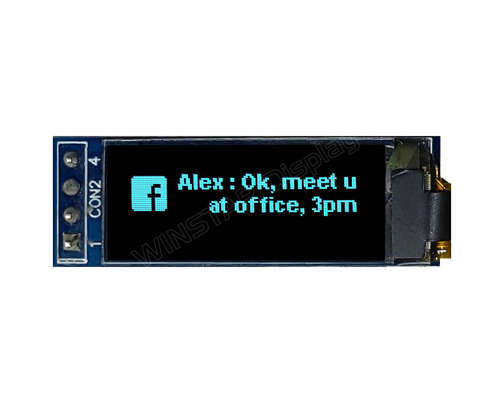
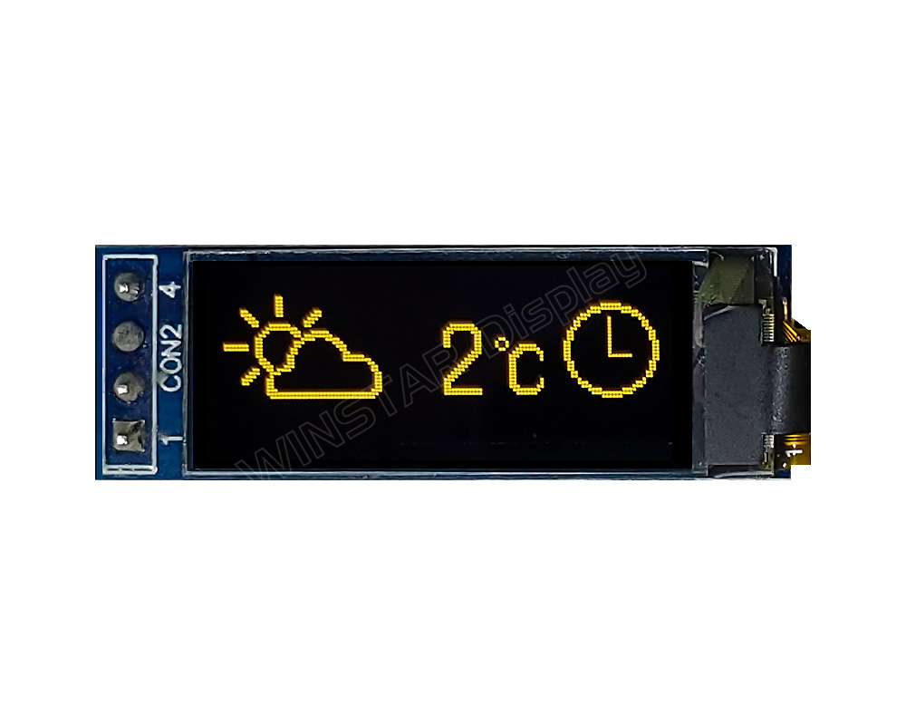
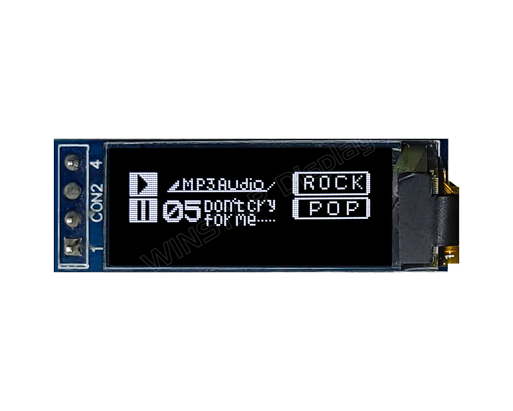
0.91 inch OLED Display Module, OLED Display 0.91 inch 128x32 (COG+PCB)

Model No. WEA012832F

►0.91 inch OLED Display Module
►Type: Graphic
►Structure: COG+PCB
►128x32 Dot Matrix
►IC:SSD1306
►3V/5V Power supply
►1/32 duty
►Interface: I2C
►Display Color: White / Yellow / Sky Blue

Description

0.91" OLED Display suitable for wearable device

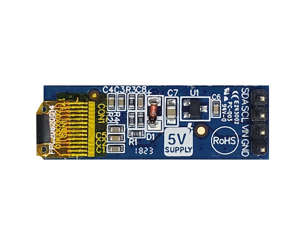
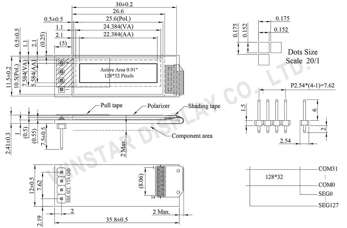
The 0.91 inch is one of the most popular sizes of COG OLED for wearable displays. WEA012832F is a graphic COG with PCB OLED module, which is made of resolution 128x32 pixels, diagonal size 0.91 inch. WEA012832F 0.91 inch OLED display module is built in with SSD1306 IC; it supports I2C interface, 1/32 driving duty. WEA012832F model is having PCB outline size 35.80 × 12.0 mm with 4x1 metal pins on module.

The supply voltage for logic of OLED display 0.91 inch WEA012832F is 3.V/ 5V, supply voltage for display is 7.5V (Internal Boots), display with 50% check board current is 13mA@3VDD (typical value). This OLED module can be operating at temperatures from -40℃ to +80℃; its storage temperatures range from -40℃ to +85℃.

DRAWING

0.91 inch OLED Display, 0.91 inch OLED Module, OLED 0.91 inch, OLED Display 0.91 128x32 - WEA012832F

Data source ref: WEA012832FLPP3N00000

SPECIFICATIONS

Mechanical Data

Item Dimension Unit
Dot Matrix 128 x 32 Dots
Module dimension 35.8 x 12.0 x 2.41 mm
Active Area 22.384 x 5.584 mm
Pixel Size 0.152 x 0.152 mm
Pixel Pitch 0.175 x 0.175 mm
Display Mode Passive Matrix
Display Color Monochrome
Drive Duty 1/32 Duty
IC SSD1306
Interface I2C
Size 0.91 inch

Absolute Maximum Ratings

Parameter Symbol Min Max Unit
Supply Voltage for Logic VIN 0 4.0 V
Operating Temperature TOP -40 +80 °C
Storage Temperature TSTG -40 +85 °C

Electronical Characteristics

DC Electrical Characteristics

Item Symbol Condition Min Typ Max Unit
Supply Voltage for Logic VIN 2.8 3.0 3.3 V
Input High Volt. VIH 0.8×VIN VIN V
Input Low Volt. VIL 0 0.2×VIN V
Output High Volt. VOH 0.9×VIN VIN V
Output Low Volt. VOL 0 0.1×VIN V
50% check Board operating Current IIN VIN=3V 13.0 26.0 mA

Interface Pin Function

No. Symbol Function
1 GND Ground
2 VIN Power supply input.
3 SCL When the I2C interface is selected, then D0 serves as the serial clock input pad (SCL) and D1 serves as the serial data input pad (SDAI).
4 SDA

Related Products

go top
close

We value your privacy

By clicking "Allow All Cookies", you agree to the storing of cookies on your device to enhance site navigation, analyse site usage, and assist in our marketing and performance efforts. You can find further information this subject in our policy.

We value your privacy

Winstar and certain third parties use cookies on www.winstar.com.tw. The details regarding the types of
cookies, their purpose and the third parties involved are described below and in our Cookie Policy.
Please click on “Allow All” to consent to our usage of cookies in order to have the best possible
experience on our websites. You can also set your preferences or reject cookies (except for strictly
necessary cookies).

Manage Consent Preferences

Always Active
Essential Cookies

These cookies are essential in order to enable you to move around the website and use its
features, such as setting your privacy preferences, logging in or filling in forms.

Analytics Cookies

Also known as “statistics cookies,” these cookies collect information about how you use a website, like which pages you visited and which links you clicked on. See Detail