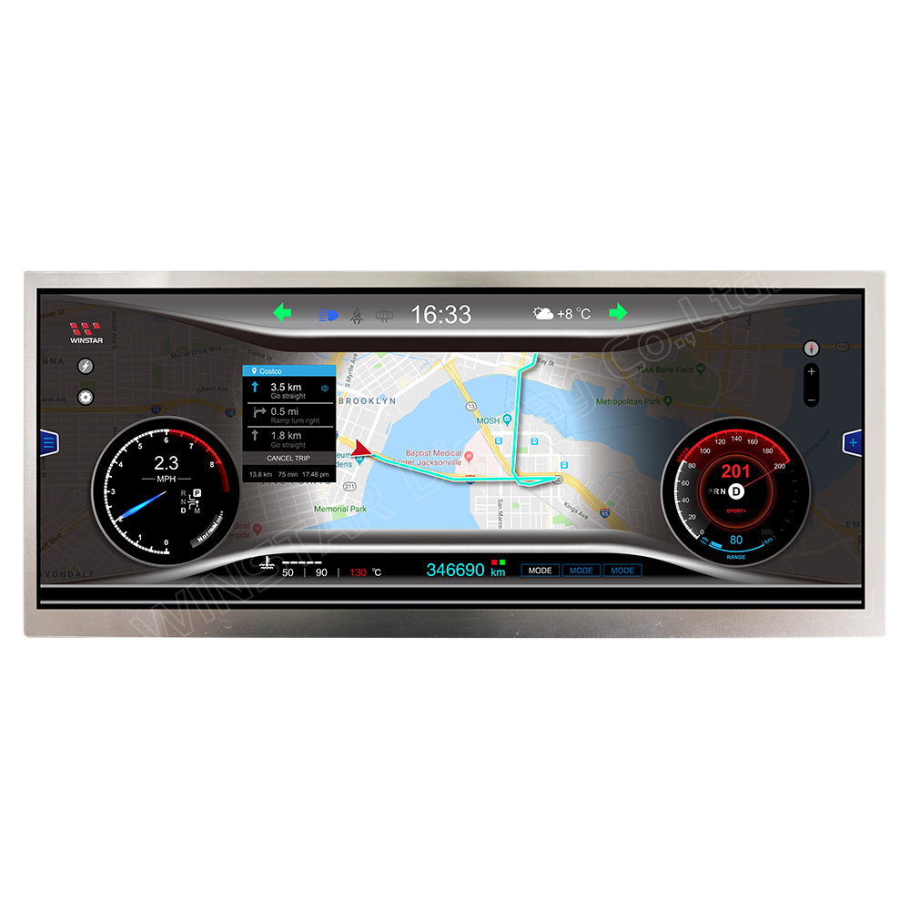
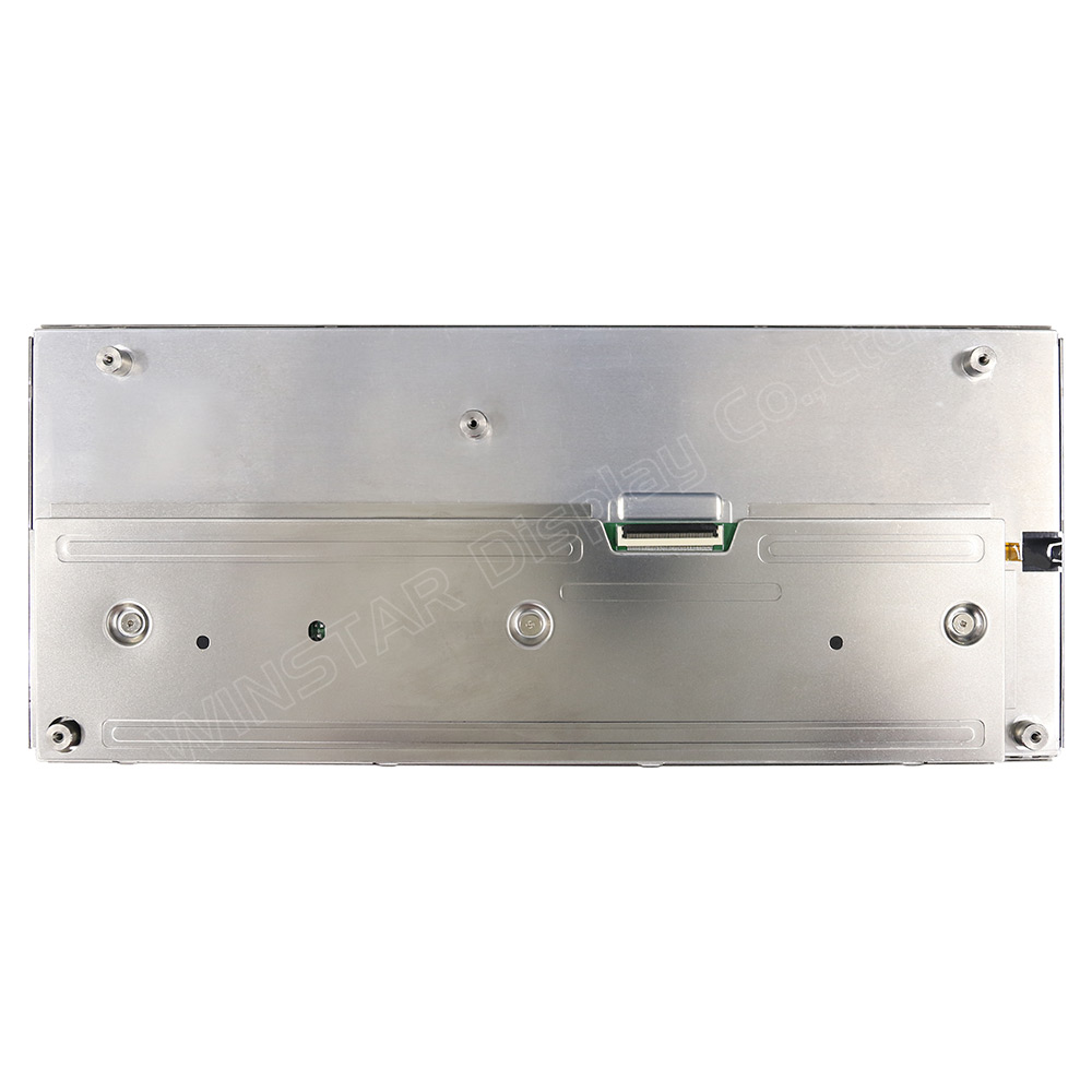
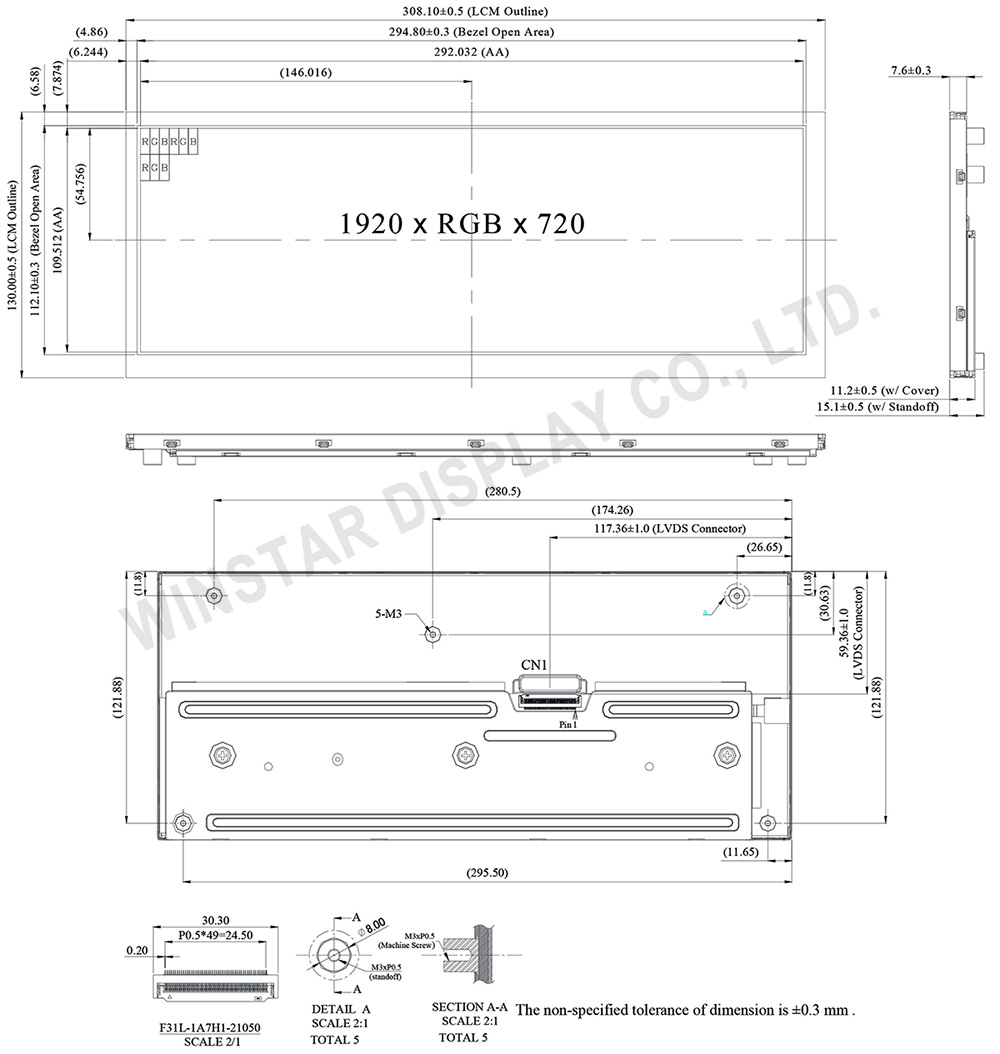
WF123BSWAYLNN0 is a high-brightness 12.3-inch IPS TFT LCD display, offering a 1920x720 resolution for crisp and clear images. It supports a 2-channel LVDS interface and delivers a typical brightness of 800 nits, along with a contrast ratio of 1,100:1. This makes it an ideal choice for both indoor and outdoor applications requiring high-quality visuals.
Thanks to the IPS technology, this 12.3-inch LCD display ensures superior color accuracy and wide viewing angles of 85° in all directions (left, right, up, and down). This feature provides excellent visibility from virtually any angle, making it suitable for a wide range of uses, from industrial controls to interactive kiosks. The anti-glare surface further enhances the user experience by minimizing reflections.
The display operates with a supply voltage (VCC) range from 3.0V to 3.6V, with a typical value of 3.3V. It can function in wide temperatures, with an operating range from -30℃ to +85℃ and a storage range from -40℃ to +90℃. The module is powered by the HX8298-C01-LT and HX8695-E-LT driver ICs, ensuring reliable performance in various settings.
The 12.3-inch TFT LCD display with 1920x720 resolution and IPS technology is perfect for applications requiring high resolution, wide viewing angles, and high brightness. With its superior color reproduction and clarity, this display stands out in any project where performance and reliability are key.
SPECIFICATIONS
General Specifications
| Item |
Dimension |
Unit |
| Size |
12.3 |
inch |
| Pixel Number |
1920 RGB (H) × 720(V) |
pixel |
| Module dimension |
308.1(H) ×130.0(V) × 7.6 |
mm |
| Active Area |
292.032(H) × 109.512(V) |
mm |
| Pixel Pitch |
0.1521(H) × 0.1521 (V) |
mm |
| LCD type |
TFT, Normally Black, Transmissive |
| TFT Driver IC |
HX8298-C01-LT+HX8695-E-LT or Equivalent |
| Viewing Angle |
85/85/85/85 |
| Backlight Type |
LED, Normally White |
| TFT Interface |
2ch-LVDS |
| Touch Panel |
Without Touch Panel |
| Surface |
Anti-Glare |
Absolute Maximum Ratings
| Item |
Symbol |
Min |
Typ |
Max |
Unit |
| Operating Temperature |
TOP |
-30 |
- |
+85 |
℃ |
| Storage Temperature |
TST |
-40 |
- |
+90 |
℃ |
Electrical Characteristics
| Item |
Symbol |
Min |
Typ |
Max |
Unit |
| Supply Voltage |
VCC |
3 |
3.3 |
3.6 |
V |
| Input signal voltage |
ViH |
VCC *0.7 |
- |
VCC |
V |
| ViL |
0 |
- |
VCC *0.3 |
V |
| Current of power supply |
ICC |
-- |
-- |
500 |
mA |
Interface
TFT LCD MODULE
FPC connector is used for electronics interface.
AORORA F31L-1A7H1-21050 , 50PIN
| Pin no. |
Symbol |
Function |
| 1 |
GND |
Ground |
| 2 |
NC |
No connector |
| 3 |
VCC |
Digital Power |
| 4 |
VCC |
Digital Power |
| 5 |
GND |
Panel Power |
| 6 |
GND |
Panel Power |
| 7 |
NC |
No connector |
| 8 |
NC |
No connector |
| 9 |
GND |
Ground |
| 10 |
ORXIN0- |
Odd pixel negative LVDS differential clock input |
| 11 |
ORXIN0+ |
Odd pixel positive LVDS differential clock input |
| 12 |
ORXIN1- |
Odd pixel negative LVDS differential clock input |
| 13 |
ORXIN1+ |
Odd pixel positive LVDS differential clock input |
| 14 |
ORXIN2- |
Odd pixel negative LVDS differential clock input |
| 15 |
ORXIN2+ |
Odd pixel positive LVDS differential clock input |
| 16 |
ORXCLKIN- |
Odd pixel negative LVDS differential clock input |
| 17 |
ORXCLKIN+ |
Odd pixel positive LVDS differential clock input |
| 18 |
ORXIN3- |
Odd pixel negative LVDS differential clock input |
| 19 |
ORXIN3+ |
Odd pixel positive LVDS differential clock input |
| 20 |
ERXIN0- |
Even pixel negative LVDS differential clock input |
| 21 |
ERXIN0+ |
Even pixel positive LVDS differential clock input |
| 22 |
ERXIN1- |
Even pixel negative LVDS differential clock input |
| 23 |
ERXIN1+ |
Even pixel positive LVDS differential clock input |
| 24 |
ERXIN2- |
Even pixel negative LVDS differential clock input |
| 25 |
ERXIN2+ |
Even pixel positive LVDS differential clock input |
| 26 |
ERXCLKIN- |
Even pixel negative LVDS differential clock input |
| 27 |
ERXCLKIN+ |
Even pixel positive LVDS differential clock input |
| 28 |
ERXIN3- |
Even pixel negative LVDS differential clock input |
| 29 |
ERXIN3+ |
Even pixel positive LVDS differential clock input |
| 30 |
GND |
Ground |
| 31 |
NC |
No connector |
| 32 |
RESETB |
Global reset pin, active low. |
| 33 |
STBYB |
Standby mode, active low. |
| 34 |
CA3 |
Output signal to indicate self protection mode, when DE,HS,VS,DCLK, any of these signals is missing, it will become High. If using this pin, CA3 need to pulled low by an resistor,else , let it floating. |
| 35 |
SCL |
Serial interface clock input. (User folating) |
| 36 |
SDA |
Serial interface data input/output.(User folating) |
| 37 |
CSB |
Serial interface chip enable.(User folating) |
| 38 |
GND |
Power Ground |
| 39 |
GND |
Power Ground |
| 40 |
NC |
No connector |
| 41 |
LEDA |
LED power (Anode) |
| 42 |
LEDA |
LED power (Anode) |
| 43 |
LEDA |
LED power (Anode) |
| 44 |
NC |
No connector |
| 45 |
LEDK1 |
Cathode 1 |
| 46 |
LEDK2 |
Cathode 2 |
| 47 |
LEDK3 |
Cathode 3 |
| 48 |
LEDK4 |
Cathode 4 |
| 49 |
NTC_A |
NTC_Anode |
| 50 |
NTC_K |
NTC_Cathode |
12.3 tft, 12.3 lcd, 1920x720 lcd, 1920x720 display, ips 12.3, 12.3 ips display


