


 - WL0F0007000A8GAAASA01")


我們重視您的隱私
通過點擊「允許所有 Cookie」,代表您同意在您的設備上存儲 Cookie 以增強網站瀏覽體驗、分析網站使用情況並協助我們的行銷和網站效能優化工作。您可以在我們的隱私權政策中找到有關於此的更多資訊。


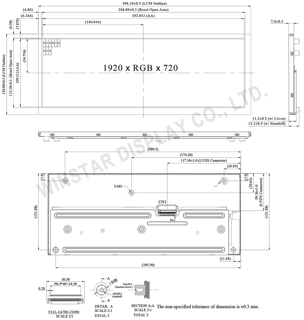
WF123BSWAYLNN0 是一款高亮度的 12.3 吋 IPS TFT LCD 顯示器,提供 1920x720 的解析度,能夠顯示清晰且細緻的影像。它支援 2 通道 LVDS 介面,並提供典型亮度 800 尼特,對比度為 1,100:1。這使得它成為需要高品質視覺效果的室內與戶外應用的理想選擇。
得益於 IPS 技術,這款 12.3 吋 LCD 顯示器保證了卓越的色彩準確度和 85° 的寬廣可視角度(左右、上下皆為 85°)。此特性提供了幾乎從任何角度的優異可視性,使其適用於各種應用,從工業控制到互動式自助終端。防眩光表面進一步提升了使用者體驗,能有效減少反射。
顯示器的供電電壓範圍為 3.0V 至 3.6V,典型值為 3.3V。它能在寬廣的溫度範圍內運行,工作溫度範圍為 -30℃ 至 +85℃,儲存溫度範圍為 -40℃ 至 +90℃。該模組由 HX8298-C01-LT 和 HX8695-E-LT 驅動 IC 提供支持,確保在各種環境下的穩定性能。
這款 12.3 吋 TFT LCD 顯示器,擁有 1920x720 解析度和 IPS 技術,非常適合需要高解析度、寬廣可視角度和高亮度的應用。憑藉其卓越的色彩重現與清晰度,這款顯示器在任何專案中都能脫穎而出,尤其是在要求高性能和高可靠性的場合。
| 項目 | 規格 | 單位 |
|---|---|---|
| 尺寸(對角線) | 12.3 | 吋 |
| 點陣(解析度) | 1920 RGB (H) × 720(V) | pixel |
| 模組尺寸 | 308.1(H) ×130.0(V) × 7.6 | mm |
| 有效區域 | 292.032(H) × 109.512(V) | mm |
| 像素間距 | 0.1521(H) × 0.1521 (V) | mm |
| LCD類型 | TFT, 平常黑, 透射式 | |
| TFT 驅動IC | HX8298-C01-LT+HX8695-E-LT 或相容IC | |
| 視角 | 85/85/85/85 | |
| 背光類型 | LED ,平常白 | |
| TFT 介面 | 2ch-LVDS | |
| 觸控面板 | 無觸控面板 | |
| 表面 | 防眩光 | |
| 項目 | 符號 | 最小值 | 典型值 | 最大值 | 單位 |
|---|---|---|---|---|---|
| 工作溫度 | TOP | -30 | - | +85 | ℃ |
| 儲存溫度 | TST | -40 | - | +90 | ℃ |
| 項目 | 符號 | 最小值 | 典型值 | 最大值 | 單位 |
|---|---|---|---|---|---|
| 電源電壓 | VCC | 3 | 3.3 | 3.6 | V |
| 輸入信號電壓 | ViH | VCC *0.7 | - | VCC | V |
| ViL | 0 | - | VCC *0.3 | V | |
| 供電電流 | ICC | -- | -- | 500 | mA |
| Pin no. | 符號 | 功能說明 |
|---|---|---|
| 1 | GND | Ground |
| 2 | NC | No connector |
| 3 | VCC | Digital Power |
| 4 | VCC | Digital Power |
| 5 | GND | Panel Power |
| 6 | GND | Panel Power |
| 7 | NC | No connector |
| 8 | NC | No connector |
| 9 | GND | Ground |
| 10 | ORXIN0- | Odd pixel negative LVDS differential clock input |
| 11 | ORXIN0+ | Odd pixel positive LVDS differential clock input |
| 12 | ORXIN1- | Odd pixel negative LVDS differential clock input |
| 13 | ORXIN1+ | Odd pixel positive LVDS differential clock input |
| 14 | ORXIN2- | Odd pixel negative LVDS differential clock input |
| 15 | ORXIN2+ | Odd pixel positive LVDS differential clock input |
| 16 | ORXCLKIN- | Odd pixel negative LVDS differential clock input |
| 17 | ORXCLKIN+ | Odd pixel positive LVDS differential clock input |
| 18 | ORXIN3- | Odd pixel negative LVDS differential clock input |
| 19 | ORXIN3+ | Odd pixel positive LVDS differential clock input |
| 20 | ERXIN0- | Even pixel negative LVDS differential clock input |
| 21 | ERXIN0+ | Even pixel positive LVDS differential clock input |
| 22 | ERXIN1- | Even pixel negative LVDS differential clock input |
| 23 | ERXIN1+ | Even pixel positive LVDS differential clock input |
| 24 | ERXIN2- | Even pixel negative LVDS differential clock input |
| 25 | ERXIN2+ | Even pixel positive LVDS differential clock input |
| 26 | ERXCLKIN- | Even pixel negative LVDS differential clock input |
| 27 | ERXCLKIN+ | Even pixel positive LVDS differential clock input |
| 28 | ERXIN3- | Even pixel negative LVDS differential clock input |
| 29 | ERXIN3+ | Even pixel positive LVDS differential clock input |
| 30 | GND | Ground |
| 31 | NC | No connector |
| 32 | RESETB | Global reset pin, active low. |
| 33 | STBYB | Standby mode, active low. |
| 34 | CA3 | Output signal to indicate self protection mode, when DE,HS,VS,DCLK, any of these signals is missing, it will become High. If using this pin, CA3 need to pulled low by an resistor,else , let it floating. |
| 35 | SCL | Serial interface clock input. (User folating) |
| 36 | SDA | Serial interface data input/output.(User folating) |
| 37 | CSB | Serial interface chip enable.(User folating) |
| 38 | GND | Power Ground |
| 39 | GND | Power Ground |
| 40 | NC | No connector |
| 41 | LEDA | LED power (Anode) |
| 42 | LEDA | LED power (Anode) |
| 43 | LEDA | LED power (Anode) |
| 44 | NC | No connector |
| 45 | LEDK1 | Cathode 1 |
| 46 | LEDK2 | Cathode 2 |
| 47 | LEDK3 | Cathode 3 |
| 48 | LEDK4 | Cathode 4 |
| 49 | NTC_A | NTC_Anode |
| 50 | NTC_K | NTC_Cathode |

通過點擊「允許所有 Cookie」,代表您同意在您的設備上存儲 Cookie 以增強網站瀏覽體驗、分析網站使用情況並協助我們的行銷和網站效能優化工作。您可以在我們的隱私權政策中找到有關於此的更多資訊。