


我們重視您的隱私
通過點擊「允許所有 Cookie」,代表您同意在您的設備上存儲 Cookie 以增強網站瀏覽體驗、分析網站使用情況並協助我們的行銷和網站效能優化工作。您可以在我們的隱私權政策中找到有關於此的更多資訊。


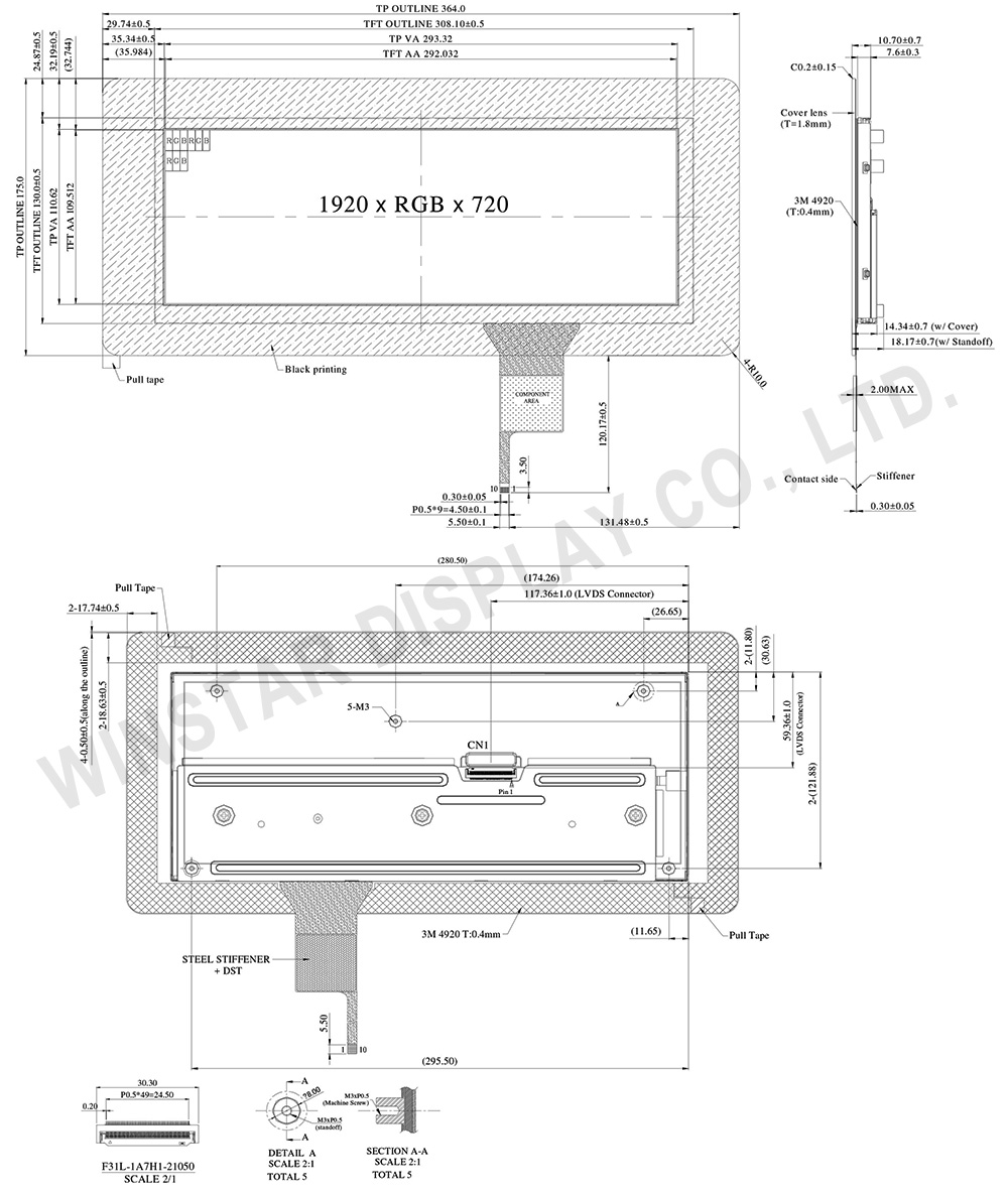
WF123BSWAYLNBA 是一款 12.3 吋觸控 TFT 顯示器,採用 IPS 技術,擁有 85/85/85/85 的廣視角,解析度為 1920x720 像素,亮度達 650 cd/m²。模組尺寸為 364.0 (H) × 175.0 (V) mm,有效區域為 292.032 (H) × 109.512 (V) mm。內建 HX8298-C01-LT+HX8695-E-LT 驅動 IC,支援 2 通道 LVDS 介面。顯示器配備投射電容觸控面板(PCAP),搭載 ILI2511 驅動 IC,能同時偵測最多 10 點觸控,並支援 USB 及 I2C 介面。
顯示器的供電電壓(VCC)範圍為 3V 至 3.6V,典型值為 3.3V。工作溫度範圍為 -30℃ 至 +85℃,儲存溫度範圍為 -40℃ 至 +90℃。
與 WF123BSWAYLNB0 相比,主要差異在於儲存溫度範圍。WF123BSWAYLNBA 支援更寬的儲存溫度範圍(-40℃ 至 +90℃),而 WF123BSWAYLNB0 的儲存範圍為 -40℃ 至 +85℃。此外,模組厚度也略有不同:
請根據需求選擇最適合的型號。
| 項目 | 規格 | 單位 |
|---|---|---|
| 尺寸(對角線) | 12.3 | 吋 |
| 點陣(解析度) | 1920 RGB (H) × 720(V) | 像素 |
| 模組尺寸 | 364.0(H) × 175.0 (V) × 10.7 | mm |
| 有效區域 | 292.032(H) × 109.512(V) | mm |
| 像素間距 | 0.1521(H) × 0.1521 (V) | mm |
| LCD類型 | TFT全透 | |
| 驅動IC | HX8298-C01-LT+HX8695-E-LT 或相容IC | |
| 視角 | 85/85/85/85 | |
| 背光類型 | LED,白色 | |
| TFT 介面 | 2ch-LVDS | |
| PCAP IC | ILI2511 或相容IC | |
| PCAP 介面 | USB (I2C available) | |
| PCAP FW 版本 | V6.0.0.0.0.0.0.3 | |
| 觸控面板 | 投射電容式觸控面板 (PCAP) | |
| 表面 | 亮面 | |
| 項目 | 符號 | 最小值 | 典型值 | 最大值 | 單位 |
|---|---|---|---|---|---|
| 工作溫度 | TOP | -30 | - | +85 | ℃ |
| 儲存溫度 | TST | -40 | - | +90 | ℃ |
| 項目 | 符號 | 最小值 | 典型值 | 最大值 | 單位 |
|---|---|---|---|---|---|
| 電源電壓 | VCC | 3 | 3.3 | 3.6 | V |
| 輸入信號電壓 | ViH | VCC *0.7 | - | VCC | V |
| ViL | 0 | - | VCC *0.3 | V | |
| 供電電流 | ICC | - | - | 500 | mA |
| 湧浪電流 | IRUSH | - | - | 2.0 | A |
| PCAP(USB)電源電壓 | USB_VDD 5V | 4.75 | 5.0 | 5.25 | V |
| I USB_VDD | - | 90 | 135 | mA | |
| PCAP(I2C)電源電壓 | VDDT 3.3 | 3.15 | 3.3 | 3.45 | V |
| IVDDT | - | 90 | 135 | mA |
| Pin no. | 符號 | 功能說明 |
|---|---|---|
| 1 | GND | Ground |
| 2 | NC | No connector |
| 3 | VCC | Digital Power |
| 4 | VCC | Digital Power |
| 5 | GND | Panel Power |
| 6 | GND | Panel Power |
| 7 | NC | No connector |
| 8 | NC | No connector |
| 9 | GND | Ground |
| 10 | ORXIN0- | Odd pixel negative LVDS differential clock input |
| 11 | ORXIN0+ | Odd pixel positive LVDS differential clock input |
| 12 | ORXIN1- | Odd pixel negative LVDS differential clock input |
| 13 | ORXIN1+ | Odd pixel positive LVDS differential clock input |
| 14 | ORXIN2- | Odd pixel negative LVDS differential clock input |
| 15 | ORXIN2+ | Odd pixel positive LVDS differential clock input |
| 16 | ORXCLKIN- | Odd pixel negative LVDS differential clock input |
| 17 | ORXCLKIN+ | Odd pixel positive LVDS differential clock input |
| 18 | ORXIN3- | Odd pixel negative LVDS differential clock input |
| 19 | ORXIN3+ | Odd pixel positive LVDS differential clock input |
| 20 | ERXIN0- | Even pixel negative LVDS differential clock input |
| 21 | ERXIN0+ | Even pixel positive LVDS differential clock input |
| 22 | ERXIN1- | Even pixel negative LVDS differential clock input |
| 23 | ERXIN1+ | Even pixel positive LVDS differential clock input |
| 24 | ERXIN2- | Even pixel negative LVDS differential clock input |
| 25 | ERXIN2+ | Even pixel positive LVDS differential clock input |
| 26 | ERXCLKIN- | Even pixel negative LVDS differential clock input |
| 27 | ERXCLKIN+ | Even pixel positive LVDS differential clock input |
| 28 | ERXIN3- | Even pixel negative LVDS differential clock input |
| 29 | ERXIN3+ | Even pixel positive LVDS differential clock input |
| 30 | GND | Ground |
| 31 | NC | No connector |
| 32 | RESETB | Global reset pin, active low. |
| 33 | STBYB | Standby mode, active low. |
| 34 | CA3 | Output signal to indicate self protection mode, when DE,HS,VS,DCLK, any of these signals is missing, it will become High. If using this pin, CA3 need to pulled low by an resistor,else , let it floating. |
| 35 | SCL | Serial interface clock input. (User folating) |
| 36 | SDA | Serial interface data input/output.(User folating) |
| 37 | CSB | Serial interface chip enable.(User folating) |
| 38 | GND | Power Ground |
| 39 | GND | Power Ground |
| 40 | NC | No connector |
| 41 | LEDA | LED power (Anode) |
| 42 | LEDA | LED power (Anode) |
| 43 | LEDA | LED power (Anode) |
| 44 | NC | No connector |
| 45 | LEDK1 | Cathode 1 |
| 46 | LEDK2 | Cathode 2 |
| 47 | LEDK3 | Cathode 3 |
| 48 | LEDK4 | Cathode 4 |
| 49 | NTC_A | NTC_Anode |
| 50 | NTC_K | NTC_Cathode |
| Pin | 符號 | 功能說明 |
|---|---|---|
| 1 | USB_VSS | System ground |
| 2 | USB_VDD 5V | Power supply |
| 3 | USB_D+ | Data + |
| 4 | USB_D- | Data - |
| 5 | VSS | System ground |
| 6 | SDA | I2C data input and output |
| 7 | SCL | I2C clock input |
| 8 | RST | External Reset, Low is active |
| 9 | INT | External interrupt to the host |
| 10 | VDDT 3.3 | Power supply |

通過點擊「允許所有 Cookie」,代表您同意在您的設備上存儲 Cookie 以增強網站瀏覽體驗、分析網站使用情況並協助我們的行銷和網站效能優化工作。您可以在我們的隱私權政策中找到有關於此的更多資訊。