
 - WF123BSWAYLNB0")
 - WL0F00043000WGAAASA00")
 - WL0F00043000WGAAESA00")


우리는 귀하의 프라이버시를 소중히 여깁니다
"모든 쿠키 허용"을 클릭하면 사이트 탐색을 개선하고, 사이트 사용을 분석하며, 마케팅 및 성능 노력에 도움을 주기 위해 쿠키를 귀하의 장치에 저장하는 데 동의한 것으로 간주됩니다. 이 주제에 대한 추가 정보는 당사의 정책에서 확인할 수 있습니다. 개인정보 보호정책


모델 번호 WF123BSWAYLNBA
►크기:12.3 인치
►디스플레이 형식:1920x720 dots
►뷰 방향 :85/85/85/85 (IPS)
►인터페이스 :2ch-LVDS
►드라이버IC :HX8298-C01-LT+HX8695-E-LT
►제어 보드 : 없음
►밝기(cd/m²): 650
►스루 홀 프레임: 없음
►터치스크린 : 용량식 터치패널이 있는 (PCAP)
►Detect Point : 10 Fingers
►작동 온도 : -30~+85℃ (넓은 온도 TFT)
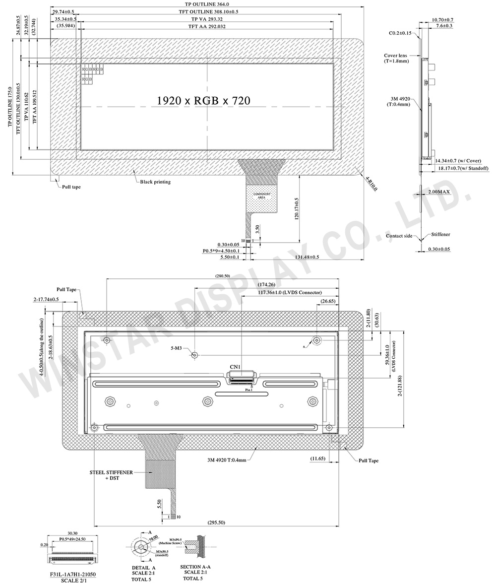
WF123BSWAYLNBA는 IPS 기술을 채택한 12.3인치 터치 TFT 디스플레이로 85/85/85/85의 넓은 시야각을 제공합니다. 해상도는 1920x720 픽셀이며, 밝기는 650 cd/m²입니다. 모듈 크기는 364.0 (H) × 175.0 (V) mm이며, 활성 영역은 292.032 (H) × 109.512 (V) mm입니다. HX8298-C01-LT+HX8695-E-LT 드라이버 IC를 장착하고 2채널 LVDS 인터페이스를 지원합니다. 디스플레이에는 ILI2511 IC가 탑재된 투과형 정전 용량식 터치 패널(PCAP)이 포함되어 있으며, 최대 10점의 터치를 동시에 감지할 수 있으며, USB 및 I2C 인터페이스를 지원합니다.
공급 전압(VCC)은 3V에서 3.6V 범위이며, 일반적인 값은 3.3V입니다. 동작 온도 범위는 -30℃에서 +85℃이며, 저장 온도 범위는 -40℃에서 +90℃입니다.
WF123BSWAYLNB0와의 주요 차이점은 저장 온도 범위입니다. WF123BSWAYLNBA는 -40℃에서 +90℃의 더 넓은 저장 온도 범위를 지원하며, WF123BSWAYLNB0는 -40℃에서 +85℃로 제한됩니다. 또한 모듈 두께에도 약간의 차이가 있습니다:
귀하의 애플리케이션에 가장 적합한 모델을 선택할 때 이러한 요소들을 고려하십시오.
| 항목 | 치수 | 단위 |
|---|---|---|
| 크기 (대각선) | 12.3 | 인치 |
| 도트 매트릭스 | 1920 RGB (H) × 720(V) | 픽셀 |
| 모듈 치수 | 364.0(H) × 175.0 (V) × 10.7 | mm |
| 활성 영역 | 292.032(H) × 109.512(V) | mm |
| 도트 피치 | 0.1521(H) × 0.1521 (V) | mm |
| LCD 유형 | TFT, 검은색, 투과성 | |
| 드라이버 IC | HX8298-C01-LT+HX8695-E-LT 또는 이와 동등한 | |
| 시야각 | 85/85/85/85 | |
| 역광 타입 | LED , 백색 | |
| TFT 인터페이스 | 2ch-LVDS | |
| PCAP IC | ILI2511 또는 이와 동등한 | |
| PCAP 인터페이스 | USB (I2C available) | |
| PCAP FW 버전 | V6.0.0.0.0.0.0.3 | |
| 터치 패널 | PCAP, 용량식 터치패널 | |
| 표면 | 눈부심 | |
| 항목 | 기호 | 최소값 | 대표값 | 최대값 | 단위 |
|---|---|---|---|---|---|
| 작동 온도 | TOP | -30 | - | +85 | ℃ |
| 보관 온도 | TST | -40 | - | +90 | ℃ |
| 항목 | 기호 | 최소값 | 대표값 | 최대값 | 단위 |
|---|---|---|---|---|---|
| Supply Voltage | VCC | 3 | 3.3 | 3.6 | V |
| Input signal voltage | ViH | VCC *0.7 | - | VCC | V |
| ViL | 0 | - | VCC *0.3 | V | |
| Current of power supply | ICC | - | - | 500 | mA |
| Inrush current | IRUSH | - | - | 2.0 | A |
| Supply PCAP (USB) | USB_VDD 5V | 4.75 | 5.0 | 5.25 | V |
| I USB_VDD | - | 90 | 135 | mA | |
| Supply PCAP (I2C) | VDDT 3.3 | 3.15 | 3.3 | 3.45 | V |
| IVDDT | - | 90 | 135 | mA |
FPC connector is used for electronics interface.
AORORA F31L-1A7H1-21050 , 50PIN
| Pin no. | 기호 | 기능 |
|---|---|---|
| 1 | GND | Ground |
| 2 | NC | No connector |
| 3 | VCC | Digital Power |
| 4 | VCC | Digital Power |
| 5 | GND | Panel Power |
| 6 | GND | Panel Power |
| 7 | NC | No connector |
| 8 | NC | No connector |
| 9 | GND | Ground |
| 10 | ORXIN0- | Odd pixel negative LVDS differential clock input |
| 11 | ORXIN0+ | Odd pixel positive LVDS differential clock input |
| 12 | ORXIN1- | Odd pixel negative LVDS differential clock input |
| 13 | ORXIN1+ | Odd pixel positive LVDS differential clock input |
| 14 | ORXIN2- | Odd pixel negative LVDS differential clock input |
| 15 | ORXIN2+ | Odd pixel positive LVDS differential clock input |
| 16 | ORXCLKIN- | Odd pixel negative LVDS differential clock input |
| 17 | ORXCLKIN+ | Odd pixel positive LVDS differential clock input |
| 18 | ORXIN3- | Odd pixel negative LVDS differential clock input |
| 19 | ORXIN3+ | Odd pixel positive LVDS differential clock input |
| 20 | ERXIN0- | Even pixel negative LVDS differential clock input |
| 21 | ERXIN0+ | Even pixel positive LVDS differential clock input |
| 22 | ERXIN1- | Even pixel negative LVDS differential clock input |
| 23 | ERXIN1+ | Even pixel positive LVDS differential clock input |
| 24 | ERXIN2- | Even pixel negative LVDS differential clock input |
| 25 | ERXIN2+ | Even pixel positive LVDS differential clock input |
| 26 | ERXCLKIN- | Even pixel negative LVDS differential clock input |
| 27 | ERXCLKIN+ | Even pixel positive LVDS differential clock input |
| 28 | ERXIN3- | Even pixel negative LVDS differential clock input |
| 29 | ERXIN3+ | Even pixel positive LVDS differential clock input |
| 30 | GND | Ground |
| 31 | NC | No connector |
| 32 | RESETB | Global reset pin, active low. |
| 33 | STBYB | Standby mode, active low. |
| 34 | CA3 | Output signal to indicate self protection mode, when DE,HS,VS,DCLK, any of these signals is missing, it will become High. If using this pin, CA3 need to pulled low by an resistor,else , let it floating. |
| 35 | SCL | Serial interface clock input. (User folating) |
| 36 | SDA | Serial interface data input/output.(User folating) |
| 37 | CSB | Serial interface chip enable.(User folating) |
| 38 | GND | Power Ground |
| 39 | GND | Power Ground |
| 40 | NC | No connector |
| 41 | LEDA | LED power (Anode) |
| 42 | LEDA | LED power (Anode) |
| 43 | LEDA | LED power (Anode) |
| 44 | NC | No connector |
| 45 | LEDK1 | Cathode 1 |
| 46 | LEDK2 | Cathode 2 |
| 47 | LEDK3 | Cathode 3 |
| 48 | LEDK4 | Cathode 4 |
| 49 | NTC_A | NTC_Anode |
| 50 | NTC_K | NTC_Cathode |
| Pin | 기호 | 기능 |
|---|---|---|
| 1 | USB_VSS | System ground |
| 2 | USB_VDD 5V | Power supply |
| 3 | USB_D+ | Data + |
| 4 | USB_D- | Data - |
| 5 | VSS | System ground |
| 6 | SDA | I2C data input and output |
| 7 | SCL | I2C clock input |
| 8 | RST | External Reset, Low is active |
| 9 | INT | External interrupt to the host |
| 10 | VDDT 3.3 | Power supply |

"모든 쿠키 허용"을 클릭하면 사이트 탐색을 개선하고, 사이트 사용을 분석하며, 마케팅 및 성능 노력에 도움을 주기 위해 쿠키를 귀하의 장치에 저장하는 데 동의한 것으로 간주됩니다. 이 주제에 대한 추가 정보는 당사의 정책에서 확인할 수 있습니다. 개인정보 보호정책