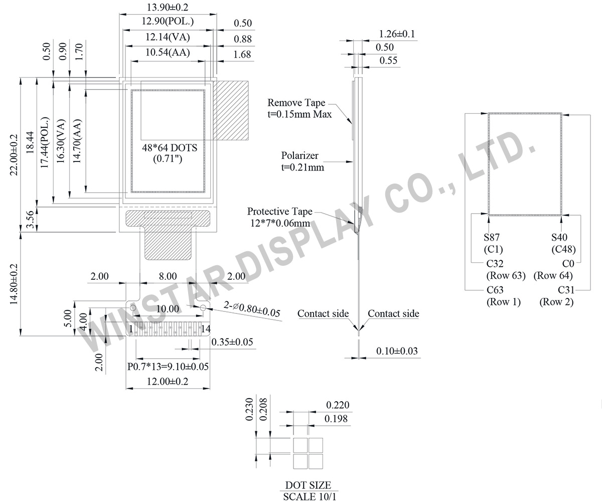
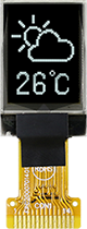
0.71 inch 48x64 Smallest OLED Display
Model No. WEO004864A
►Type: Graphic
►Structure: COG
►Size: 0.71 inch OLED Display
►48 x 64 Dot Matrix
►IC:SSD1306
►3V Power supply
►1/64 duty
►Interface: I2C
►Display Color: White / Yellow
►Suitable for Wearable Device
►Other FPC options available in below table
Description
WEO004864A is a smallest OLED display which is made of 48x64 dots, diagonal size 0.71 inch. WEO004864A has the module dimension of 13.90 × 22.0 mm and Active Area size 10.54×14.70 mm; it is built in with SSD1306 controller IC; it supports I2C interface, 3V power supply. The WEO004864A is a COG structure PMOLED display which is ultra thin and no need of backlight (self emitting); it's lightweight and low power consumption. This 0.71 inch 48x64 smallest OLED display is suitable for wearable device, mp3, portable device, personal care appliance, voice recorder pen, health device, etc. This 0.71” WEO004864A module is portrait mode; it also support landscape mode, welcome to contact us for more technical support.
WEO004864A module can be operating at temperatures from -40℃ to +80℃; its storage temperatures range from -40℃ to +85℃. Below is the basic specification of WEO004864A as reference.
FPC Options
DRAWING
Data source ref: WEO004864AWPP3N00000
SPECIFICATIONS
Interface Pin Function
No. | Symbol | Function |
---|---|---|
1 | C2N | Positive Terminal of the Flying Inverting Capacitorr Negative Terminal of the Flying Boost Capacitor The charge-pump capacitors are required between the terminals. They must be floated when the converter is not used. |
2 | C2P | |
3 | C1P | |
4 | C1N | |
5 | VBAT | Power Supply for DC/DC Converter Circuit This is the power supply pin for the internal buffer of the DC/DC voltage converter. It must be connected to external source when the converter is used. It should be connected to VDD when the converter is not used. |
6 | NC | No connection. |
7 | VSS | Ground of Logic Circuit This is a ground pin. It acts as a reference for the logic pins. It must be connected to external ground. |
8 | VDD | Power Supply for Logic This is a voltage supply pin. It must be connected to external source. |
9 | RES# | Power Reset for Controller and Driver This pin is reset signal input. When the pin is low, initialization of the chip is executed. |
10 | SCL | Host Data Input/Output Bus When serial mode is selected, D1 will be the serial data input SDIN and D0 will be the serial clock input SCLK. When I2C mode is selected, D2 & D1 should be tired together and serve as SDAout & SDAin in application and D0 is the serial clock input SCL. |
11 | SDA | |
12 | IREF | This is segment output current reference pin. When external IREF is used, a resistor should be connected between this pin and Vss to maintain the IREF current at a maximum of 30uA. When internal IREF is used, this pin should be kept NC |
13 | VCOMH | Voltage Output High Level for COM Signal This pin is the input pin for the voltage output high level for COM signals. A capacitor should be connected between this pin and VSS. |
14 | VCC | Power Supply for OEL Panel This is the most positive voltage supply pin of the chip. A stabilization capacitor should be connected between this pin and VSS when the converter is used. It must be connected to external source when the converter is not used. |
Mechanical Data
Item | Dimension | Unit |
---|---|---|
Dot Matrix | 48 × 64 Dots | - |
Module dimension | 13.90 × 22.0 × 1.26 | mm |
Active Area | 10.54 × 14.70 | mm |
Pixel Size | 0.198 × 0.208 | mm |
Pixel Pitch | 0.220 × 0.230 | mm |
Display Mode | Passive Matrix | |
Display Color | Monochrome | |
Drive Duty | 1/64 Duty | |
IC | SSD1306 | |
Interface | I2C | |
Size | 0.71 inch |
Absolute Maximum Ratings
Parameter | Symbol | Min | Max | Unit |
---|---|---|---|---|
Supply Voltage for Logic | VDD | 0 | 4 | V |
Supply Voltage for Display | VCC | 0 | 15 | V |
Operating Temperature | TOP | -40 | +80 | °C |
Storage Temperature | TSTG | -40 | +85 | °C |
Electronical Characteristics
Item | Symbol | Condition | Min | Typ | Max | Unit |
Supply Voltage for Logic | VDD | - | 1.65 | 3.0 | 3.3 | V |
Supply Voltage for Display (Supplied Externally) |
VCC | - | 6.0 | 7.5 | 8.0 | V |
Charge Pump Regulator Supply Voltage | VBAT | - | 3.0 | - | 4.2 | V |
Charge Pump Output Voltage for Display (Generated by Internal DC/DC) | Charge Pump VCC |
- | 7.0 | 7.5 | - | V |
Input High Volt. | VIH | - | 0.8×VDD | - | VDD | V |
Input Low Volt. | VIL | - | 0 | - | 0.2×VDD | V |
Output High Volt. | VOH | - | 0.9×VDD | - | VDD | V |
Output Low Volt. | VOL | - | 0 | - | 0.1×VDD | V |
Display 50% Pixel on (VCC Supplied Externally) | ICC | VCC=7.5V | - | 10.0 | 15.0 | mA |
Display 50% Pixel on (VCC Generated by Internal DC/DC) |
IBAT | - | - | 15.0 | 25.0 | mA |
FPC Options:
Drawing | FPC Length | PIN | pitch | ZIF FPC or HOTBAR FPC | Interface | FPC No. | Create Date |
---|---|---|---|---|---|---|---|
16.0 | 14 | 0.7 | HOTBAR FPC | I2C | FPC2000701401XXXXX00 | 20160603 | |
11.2 | 14 | 0.7 | HOTBAR FPC | I2C | FPC2070001401XXXXX02 | 20180307 |
Search keyword: 48x64 oled, oled 48x64, 0.71 oled, 0.71" oled, 0.71 inch oled, oled 0.71 , oled 0.71"