 - WEA004864A")
我们重视您的隐私
通过点击「允许所有 Cookie」,代表您同意在您的设备上存储 Cookie 以增强网站浏览体验、分析网站使用情况并协助我们的营销和网站效能优化工作。您可以在我们的隐私权政策中找到有关于此的更多信息。


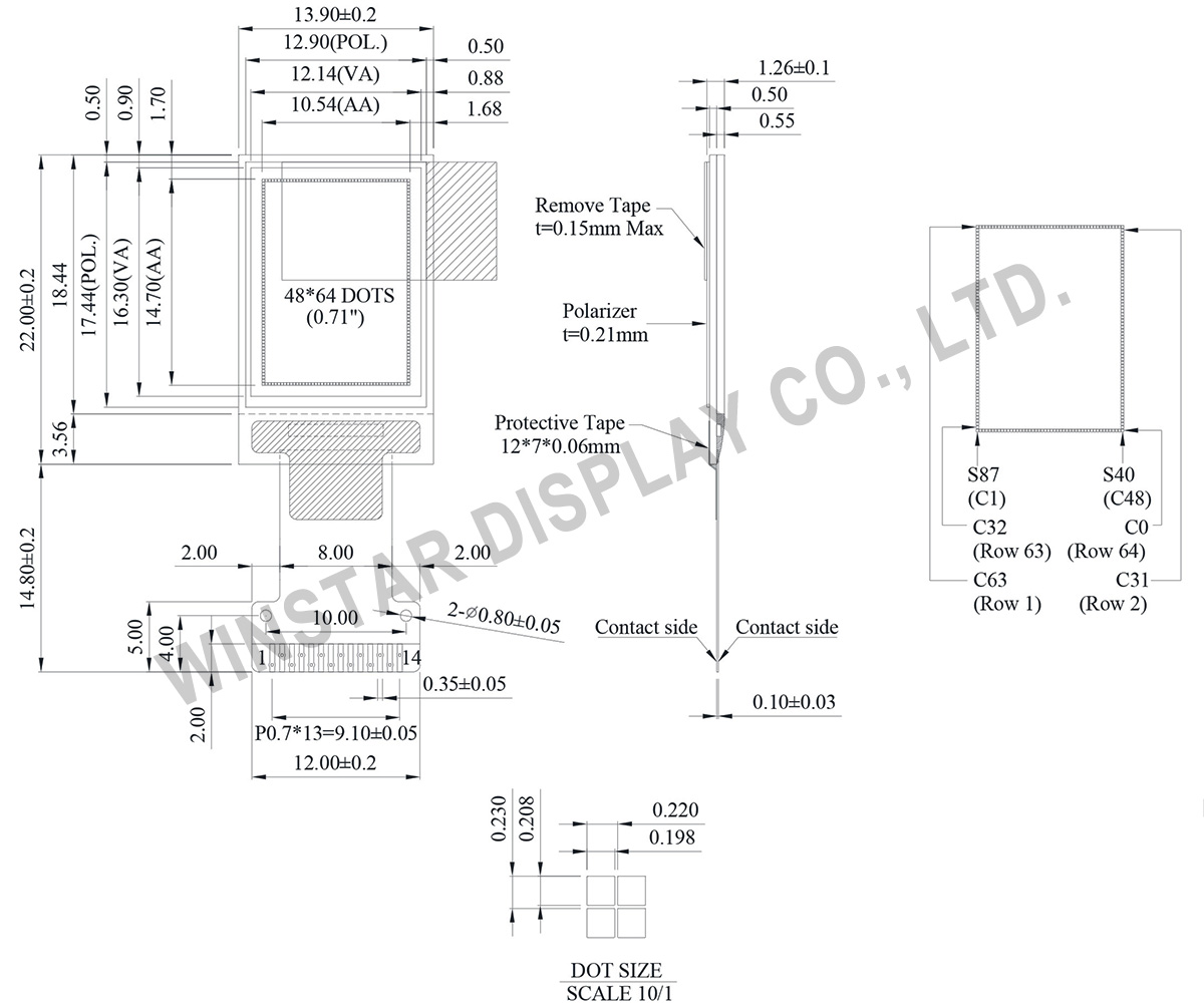
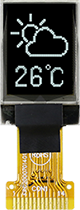
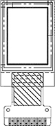
WEO004864A是一款0.71英寸窄边框超薄微型OLED显示器,解析度为48x64点阵的单色PMOLED显示模块。该模块的尺寸为13.90 × 22.0 mm,有效区域尺寸为10.54 × 14.70 mm。WEO004864A内置SSD1306控制器,并支持I2C传输接口,使用3V电压驱动。模块的工作温度范围为-40℃至+80℃,存储温度范围为-40℃至+85℃。该模块支持竖屏模式及横屏模式,提供更多灵活性。
WEO004864A采用薄型COG结构的48x64 OLED显示模块,具备有机自发光特性,无需背光源,设计轻巧且具低功耗特性。模块的厚度仅为1.26 mm,非常适合需要极致空间利用的应用。此款0.71英寸OLED模块尤为适用于穿戴设备、手环、MP3播放器、录音笔、手持设备、个人健康监测设备、儿童或老年人GPS定位设备等。
在技术规格方面,WEO004864A模块采用高性能SSD1306控制器,支持1/64 Duty。其最高可达7.5V的显示供电电压可以通过内建的升压电路或外部VCC提供,提供更多供电灵活性。显示模式为被动矩阵,显示颜色为单色,像素间距为0.220 × 0.230 mm。此外,模块的像素尺寸为0.198 × 0.208 mm。
WEO004864A的低功耗设计,使其非常适用于便携式或穿戴型设备,且具备耐用的工作温度范围,能够在各种环境下稳定运行。无论是用于可穿戴设备、医疗监测装置,还是健康追踪系统,它都能提供清晰、稳定的显示效果。
欢迎联系我们获取更多技术支持或定制选项。
 可选 FPC
| 项目 | 尺寸 | 单位 |
|---|---|---|
| 点阵(分辨率) | 48 x 64 | Dots |
| 模块尺寸 | 13.90 x 22.0 x 1.26 | mm |
| 有效区域 | 10.54 x14.70 | mm |
| 点间距 | 0.198 x 0.208 | mm |
| 点大小 | 0.220 x 0.230 | mm |
| 显示模式 | 被动矩阵 | |
| 发光颜色 | 单色 | |
| 驱动方式 | 1/64 Duty | |
| IC | SSD1306 | |
| 接口 | I2C | |
| 尺寸 | 0.71 寸 | |
| 参数 | 符号 | 最小值 | 最大值 | 单位 |
|---|---|---|---|---|
| 逻辑电源电压 | VDD | 0 | 4 | V |
| 显示电源电压 | VCC | 0 | 15 | V |
| 工作温度 | TOP | -40 | +80 | °C |
| 储存温度 | TSTG | -40 | +85 | °C |
| 项目 | 符号 | 条件 | 最小值 | 典型值 | 最大值 | 单位 |
|---|---|---|---|---|---|---|
| 逻辑电源电压 | VDD | - | 1.65 | 3.0 | 3.3 | V |
| 显示电源电压 (由外部提供) |
VCC | - | 6.0 | 7.5 | 8.0 | V |
| 电荷帮浦稳压器电源电压 | VBAT | - | 3.0 | - | 4.2 | V |
|
显示器的电荷帮浦输出电压(Generated by Internal DC/DC) |
Charge Pump VCC |
- | 7.0 | 7.5 | - | V |
| 输入高电压 | VIH | - | 0.8×VDD | - | VDD | V |
| 输入低电压 | VIL | - | 0 | - | 0.2×VDD | V |
| 输出高电压. | VOH | - | 0.9×VDD | - | VDD | V |
| 输出低电压 | VOL | - | 0 | - | 0.1×VDD | V |
| Display 50% Pixel on (VCC 由外部提供) | ICC | VCC=7.5V | - | 10.0 | 15.0 | mA |
| Display 50% Pixel on (VCC Generated by Internal DC/DC) |
IBAT | - | - | 15.0 | 25.0 | mA |
| No. | 符号 | 功能说明 |
|---|---|---|
| 1 | C2N | Positive Terminal of the Flying Inverting Capacitorr Negative Terminal of the Flying Boost Capacitor The charge-pump capacitors are required between the terminals. They must be floated when the converter is not used. |
| 2 | C2P | |
| 3 | C1P | |
| 4 | C1N | |
| 5 | VBAT | Power Supply for DC/DC Converter Circuit This is the power supply pin for the internal buffer of the DC/DC voltage converter. It must be connected to external source when the converter is used. It should be connected to VDD when the converter is not used. |
| 6 | NC | No connection. |
| 7 | VSS | Ground of Logic Circuit This is a ground pin. It acts as a reference for the logic pins. It must be connected to external ground. |
| 8 | VDD | Power Supply for Logic This is a voltage supply pin. It must be connected to external source. |
| 9 | RES# | Power Reset for Controller and Driver This pin is reset signal input. When the pin is low, initialization of the chip is executed. |
| 10 | SCL | Host Data Input/Output Bus When serial mode is selected, D1 will be the serial data input SDIN and D0 will be the serial clock input SCLK. When I2C mode is selected, D2 & D1 should be tired together and serve as SDAout & SDAin in application and D0 is the serial clock input SCL. |
| 11 | SDA | |
| 12 | IREF | This is segment output current reference pin. When external IREF is used, a resistor should be connected between this pin and Vss to maintain the IREF current at a maximum of 30uA. When internal IREF is used, this pin should be kept NC |
| 13 | VCOMH | Voltage Output High Level for COM Signal This pin is the input pin for the voltage output high level for COM signals. A capacitor should be connected between this pin and VSS. |
| 14 | VCC | Power Supply for OEL Panel This is the most positive voltage supply pin of the chip. A stabilization capacitor should be connected between this pin and VSS when the converter is used. It must be connected to external source when the converter is not used. |
| 图 | FPC 长度 | PIN | pitch | ZIF FPC 或 HOTBAR FPC | 接口 | FPC No. | 建立日期 |
|---|---|---|---|---|---|---|---|
 |
16.0 | 14 | 0.7 | HOTBAR FPC | I2C | FPC2000701401XXXXX00 | 20160603 |
 |
11.2 | 14 | 0.7 | HOTBAR FPC | I2C | FPC2070001401XXXXX02 | 20180307 |

通过点击「允许所有 Cookie」,代表您同意在您的设备上存储 Cookie 以增强网站浏览体验、分析网站使用情况并协助我们的营销和网站效能优化工作。您可以在我们的隐私权政策中找到有关于此的更多信息。