


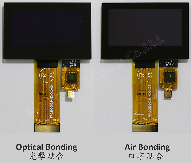
128x64 Optical Bonding OLED Touch Display, Air Bonding OLED Touch Display
Model No. WEO012864A-CTP
►Type: Graphic
►Structure: COG
►Size: 1.54"
►128 x 64 Dot Matrix
►IC:SSD1309
►3V Power supply
►1/64 duty
►Interface: 6800,8080,I2C,SPI
►With Capacitive Touch Screen (CTP); CTP Optional for Air Bonding or Optical Bonding
►Detect Point : 1 Finger
►Display Color: White / Yellow / Green
Description
WEO012864A-CTP is a 1.54-inch COG structure Graphic OLED display with Capacitive Touch Panel on the module, resolution 128x64 pixels. This module is built-in with SSD1309 IC; it can be communicated via 6800/8080 8-bit parallel, 4-wire SPI, and I2C interface; supply voltage for logic is from 2.8V to 3.3V, typical value 3.0V, the supply voltage for display 12.5V, 1/64 driving duty. We provide two CTP options for this WEO012864A-CTP model; one CTP touch panel is by Air Bonding process, and the other CTP option is by Optical Bonding (OCA) process. These two CTP touch panel options are both built-in with FT6336U IC and support I2C interface with one detect point.
WEO012864A with the CTP model is ideal for smart home applications, intelligent technology devices, meter devices, industrial control systems, medical instruments, etc. This module can be operating at temperatures from -10℃ to +60℃; its storage temperatures range from -20℃ to +70℃.
The WEO012864A-CTP model OLED module features a high contrast ratio of 10,000:1, allowing for more vibrant and deeper blacks, and brighter whites. This results in enhanced image quality, sharper details, and improved readability.
DRAWING
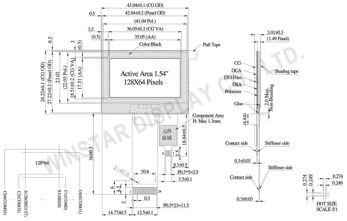
Data source ref: WEO012864AWPP3D00001
SPECIFICATIONS
Interface Pin Function
| No. | Symbol | Function | |||||||||||||||
|---|---|---|---|---|---|---|---|---|---|---|---|---|---|---|---|---|---|
| 1 | NC(GND) | No connection | |||||||||||||||
| 2 | VLSS | This is an analog ground pin | |||||||||||||||
| 3 | VSS | Ground. | |||||||||||||||
| 4 | NC | No connection | |||||||||||||||
| 5 | VDD | Power supply pin for core logic operation | |||||||||||||||
| 6 | BS1 | MCU bus interface selection pins. Select appropriate logic setting as described in the following table. BS2 and BS1 are pin select
(1) 0 is connected to VSS (2) 1 is connected to VDD |
|||||||||||||||
| 7 | BS2 | ||||||||||||||||
| 8 | CS# | This pin is the chip select input connecting to the MCU. The chip is enabled for MCU communication only when CS# is pulled LOW (active LOW). |
|||||||||||||||
| 9 | RES# | This pin is reset signal input. When the pin is pulled LOW, initialization of the chip is executed. Keep this pin pull HIGH during normal operation. |
|||||||||||||||
| 10 | D/C# | This pin is Data/Command control pin connecting to the MCU. When the pin is pulled HIGH, the data at D[7:0] will be interpreted as data. When the pin is pulled LOW, the data at D[7:0] will be transferred to a command register. In I2C mode, this pin acts as SA0 for slave address selection. |
|||||||||||||||
| 11 | R/W# | This pin is read / write control input pin connecting to the MCU interface. When 6800 interface mode is selected, this pin will be used as Read/Write (R/W#) selection input. Read mode will be carried out when this pin is pulled HIGH and write mode when LOW. When 8080 interface mode is selected, this pin will be the Write (WR#) input. Data write operation is initiated when this pin is pulled LOW and the chip is selected. When serial or I2C interface is selected, this pin must be connected to VSS. |
|||||||||||||||
| 12 | E/RD# | This pin is MCU interface input. When 6800 interface mode is selected, this pin will be used as the Enable (E) signal. Read/write operation is initiated when this pin is pulled HIGH and the chip is selected. When 8080 interface mode is selected, this pin receives the Read (RD#) signal. Read operation is initiated when this pin is pulled LOW and the chip is selected. When serial or I2C interface is selected, this pin must be connected to VSS. |
|||||||||||||||
| 13-20 | D0~D7 | These pins are bi-directional data bus connecting to the MCU data bus. Unused pins are recommended to tie LOW. When serial interface mode is selected, D0 will be the serial clock input: SCLK; D1 will be the serial data input: SDIN and D2 should be kept NC. When I2C mode is selected, D2, D1 should be tied together and serve as SDAout, SDAin in application and D0 is the serial clock input, SCL. |
|||||||||||||||
| 21 | IREF | This pin is the segment output current reference pin. IREF is supplied externally. |
|||||||||||||||
| 22 | VCOMH | COM signal deselected voltage level. A capacitor should be connected between this pin and VSS. |
|||||||||||||||
| 23 | VCC | Power supply for panel driving voltage. This is also the most positive power voltage supply pin. | |||||||||||||||
| 24 | NC(GND) | No connection |
CTP Pin Function
| 1 | GND | Ground |
| 2 | VDD | Power Supply Voltage of CTP |
| 3 | RST | External Reset, Low is active |
| 4 | INT | External interrupt to the host |
| 5 | SCL | I2C clock input |
| 6 | SDA | I2C data input and output |
Mechanical Data
| Item | Dimension | Unit |
|---|---|---|
| Dot Matrix | 128 x 64 | - |
| Module dimension | 43.04 × 28.22 × 3.01 | mm |
| Active Area | 35.05 × 17.51 | mm |
| Pixel Size | 0.249 × 0.249 | mm |
| Pixel Pitch | 0.274 × 0.274 | mm |
| Display Mode | Passive Matrix | |
| Display Color | Monochrome | |
| Drive Duty | 1/64 Duty | |
| IC | SSD1309 | |
| Interface | 6800,8080,4-wire SPI,I2C | |
| Size | 1.54 inch | |
| CTP IC | FT6336U | |
| Detect Point | 1 | |
| CTP Interface | I2C | |
| Surface | Normal Glare | |
Absolute Maximum Ratings
| Parameter | Symbol | Min | Max | Unit |
|---|---|---|---|---|
| Supply Voltage for Logic | VDD | -0.3 | 4 | V |
| Supply Voltage for Display | VCC | 0 | 17 | V |
| Operating Temperature | TOP | -10 | +60 | °C |
| Storage Temperature | TSTG | -20 | +70 | °C |
Touch Panel Controller FT6336U
| Parameter | Symbol | Min | Max | Unit |
|---|---|---|---|---|
| Power Supply Voltage | VDD | 0 | 3.6 | V |
Electrical Characteristics
DC Electrical Characteristics
| Item | Symbol | Condition | Min | Typ | Max | Unit |
|---|---|---|---|---|---|---|
| Supply Voltage for Logic | VDD | - | 2.8 | 3.0 | 3.3 | V |
| Supply Voltage for Display | VCC | - | 7.0 | 12.5 | 13.0 | V |
| High Level Input | VIH | - | 0.8×VDD | - | - | V |
| Low Level Input | VIL | - | - | - | 0.2×VDD | V |
| High Level Output | VOH | - | 0.9×VDD | - | - | V |
| Low Level Output | VOL | - | - | - | 0.1×VDD | V |
| 50% Check Board operating Current | VCC =12.5V | - | 15 | 30 | mA | |
Touch Panel Controller FT6336U
| Item | Symbol | Condition | Min | Typ | Max | Unit |
|---|---|---|---|---|---|---|
| Supply Voltage | VDD | - | 2.8 | 3.0 | 3.3 | V |
| Input High Volt. | VIH | - | 0.7×VDD | - | VDD | V |
| Input Low Volt. | VIL | - | -0.3 | - | 0.3×VDD | V |
| Output High Volt. | VOH | - | 0.7×VDD | - | - | V |
| Output Low Volt. | VOL | - | - | - | 0.3×VDD | V |
| Picture | Part Number | OLED IC | OLED Interface | TP IC | TP Interface | TP Detect Point | TP bonding method |
|---|---|---|---|---|---|---|---|
 |
WEO012864AWPP3A00000 | SSD1309 | 6800,8080,4-wire SPI,I2C | FT6336U | I2C | 1 | OCA Optical-Bonding |
 |
WEO012864AWPP3D00001 | SSD1309 | 6800,8080,4-wire SPI,I2C | FT6336U | I2C | 1 | Air-Bonding |
Search keyword: 128x64 oled, oled 128x64, 1.54 oled, 1.54" oled, 1.54 inch oled, oled 1.54"
