Home Products TFT Display Standard TFT Color Display WF70A7TIAHLNB0

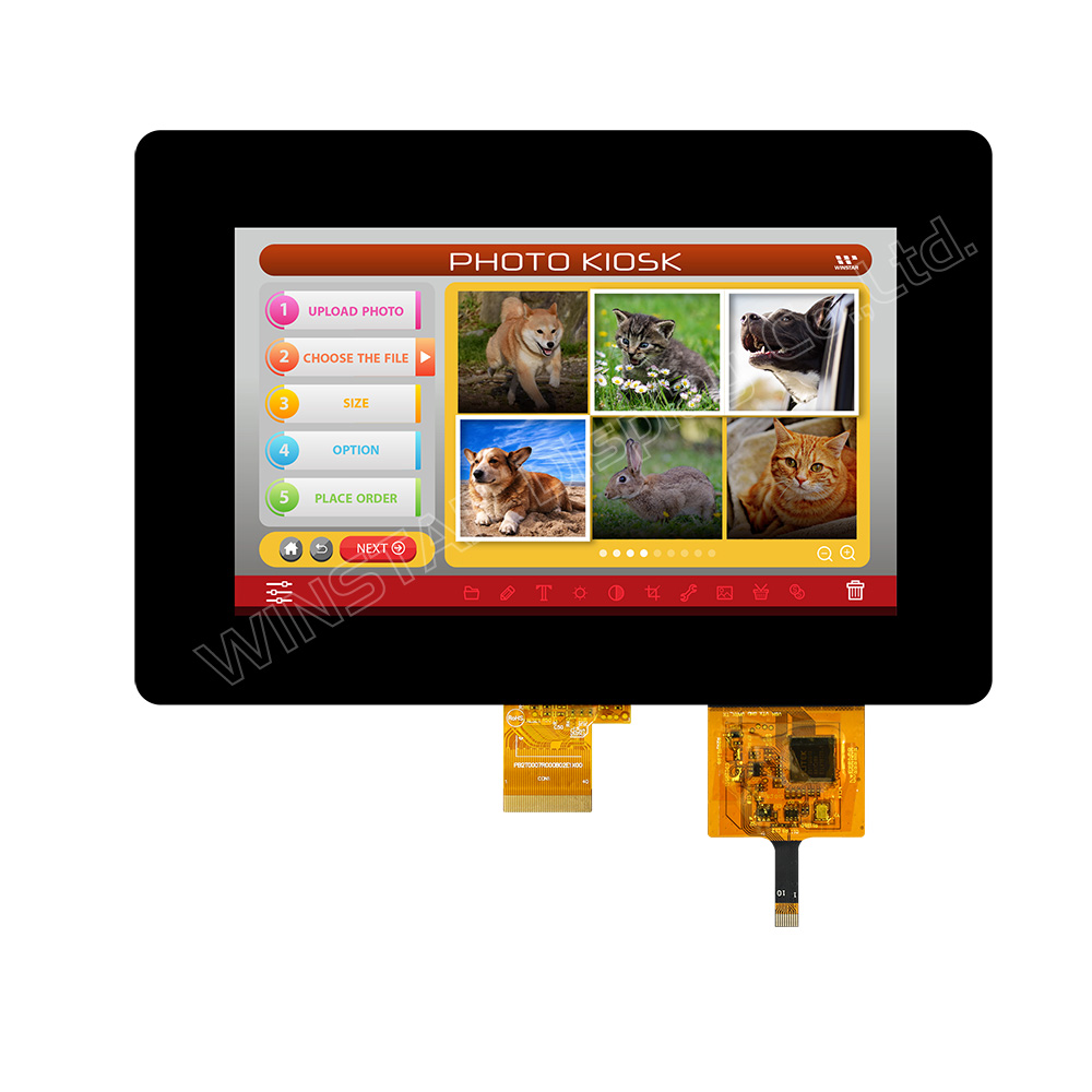
1024x600 Display with Capacitive Touch, 7-inch

Model No. WF70A7TIAHLNB0

►1024x600 Display
►Size : 7”
►View Direction : 12H
►Interface : LVDS
►Driver IC:EK79001HE + EK73215BCGA
►Control-Board : No
►Brightness(cd/m2): 450
►Frame Through Hole : No
►Touch Screen : Projected capacitive touch screen (PCAP)
►PCAP Interface : USB (I2C available)

Description

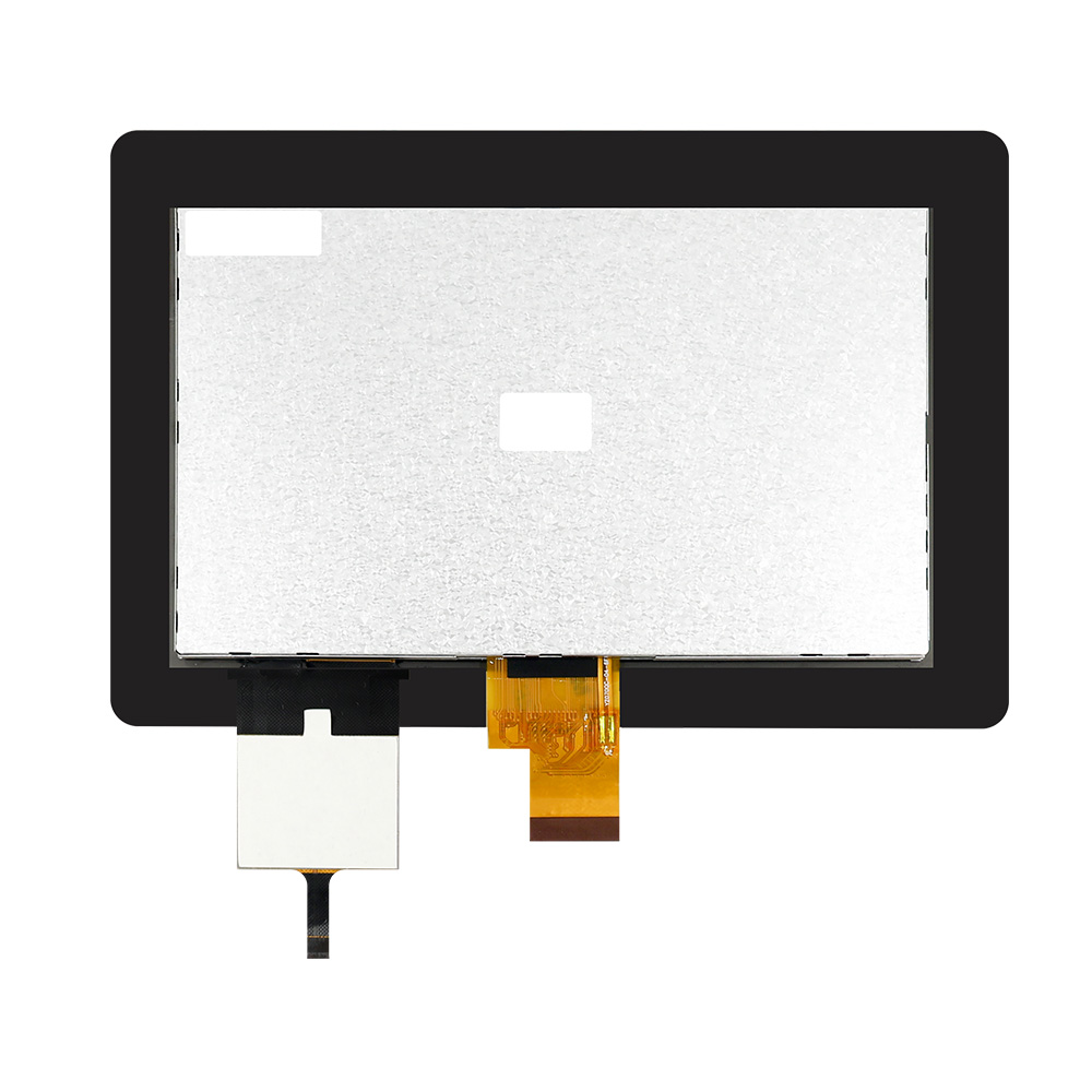
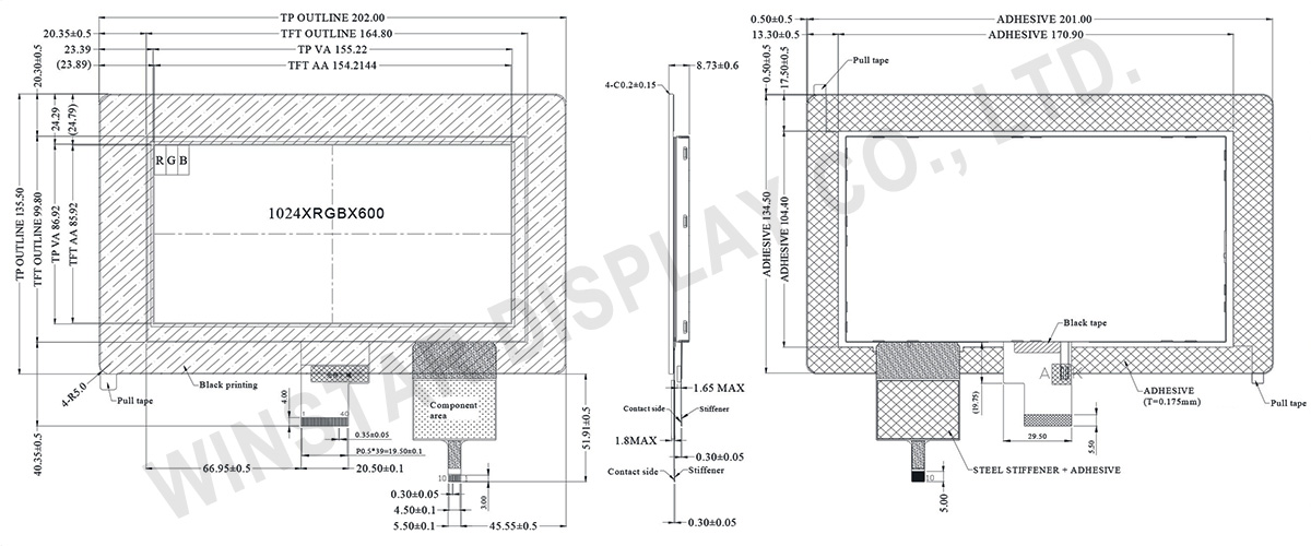
WF70A7TIAHLNB0 is a 7-inch TFT display with a resolution of 1024x600 pixels, featuring a capacitive touch screen. This 1024x600 display module supports an LVDS interface, and the capacitive touch panel is integrated with an ILI2511 driver IC, which supports USB interface (I2C available) and 10-point touch functionality.

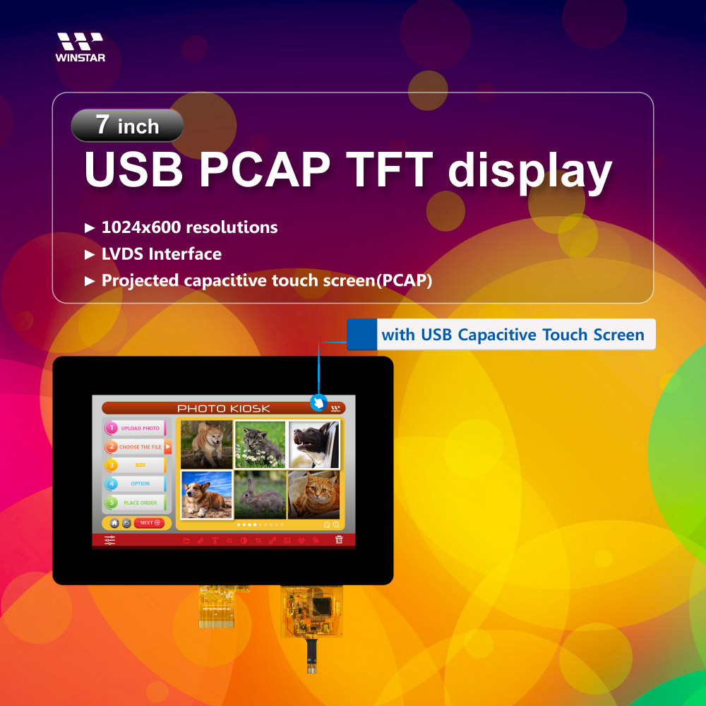
The outline dimensions of the TFT are 164.80x99.8 mm, while those of the capacitive touch screen are 202x135.50 mm, with an active area size of 154.2144x85.92 mm. To align with market trends, the cover lens dimensions are designed to be larger than the TFT module.

This TFT model has a typical brightness of 450 cd/m2 and a supply voltage (DVDD) range from 3V to 3.6V. It features a glare surface panel, with a viewing direction at 12 o'clock and grayscale inversion at 6 o'clock, and has an aspect ratio of 16:9. Operating temperatures range from -20 to +70 ℃, with storage temperatures from -30 to +80 ℃.

This 7-inch 1024x600 display is suitable for various industrial devices, smart home applications, medical equipment, testing equipment, etc.

DRAWING

1024x600 Display, USB PCAP TFT Display 7 - WF70A7TIAHLNB0 - Winstar Display

SPECIFICATIONS

General Specifications

Item Dimension Unit
Size 7.0 inch
Dot Matrix 1024 × RGB × 600(TFT) dots
Module dimension 202.0 (W) × 135.5 (H) × 8.73 (D) mm
Active area 154.2144 × 85.92 mm
Dot pitch 0.1506× 0.1432 mm
LCD type TFT, Normally White, Transmissive
View Direction 12 o'clock
Gray Scale Inversion Direction 6 o'clock
Aspect Ratio 16:9
Control IC --
TFT Driver IC EK79001HE + EK73215BCGA
TFT Interface LVDS
Backlight Type LED, Normally White
Touch Panel PCAP
PCAP IC ILI2511 or equivalent
PCAP Interface USB (I2C available)
PCAP FW Version V 6. 0. 0. 0. 7.65. 0. 1
Surface Glare

Absolute Maximum Ratings

Item Symbol Min Typ Max Unit
Operating Temperature TOP -20 +70
Storage Temperature TST -30 +80

Electrical Characteristics

Typical Operation Conditions

Item Symbol Values Unit
Min Typ Max
Power voltage DVDD 3.0 3.3 3.6 V
AVDD 9.4 9.6 9.8 V
VGH 17 18 19 V
VGL -6.6 -6.0 -5.4 V
Supply Voltage For Touch
Logic
VDDT 4.4 5.0 5.5 V
Input signal voltage VCOM 3.1 3.3 3.6 V
Input logic high voltage VIH 0.7 DVDD - DVDD V
Input logic low voltage VIL 0 - 0.3 DVDD V

Current Consumption

Item Symbol Values Unit
Min. Typ. Max.
Current for Driver IGH - 0.2 1.0 mA
IGL - 0.2 1.0 mA
IDVDD - 4.0 10 mA
IAVDD - 20 50 mA

Backlight Driving Conditions

Item Symbol Values Unit
Min. Typ. Max.
Voltage for LED backlight VL 8.4 9.8 10.8 V
Current for LED backlight IL -- 300 -- mA
LED life time - - 50,000 - Hr

Interface Pin Function

LCM PIN Definition

Pin No. Symbol I/O Function
1 VCOM P Common Voltage
2 VDD P Digital circuit
3 VDD P Digital circuit
4 NC --- No connection
5 Reset I Global reset pin
6 STBYB I Standby mode, Normally pulled high
STBYB = “1”, normal operation
STBYB = “0”, timing controller, source driver will turn off, all output are High-Z
7 GND P Ground
8 RXIN0- I Negative LVDS differential data input
9 RXIN0+ I Positive LVDS differential data input
10 GND P Ground
11 RXIN1- I Negative LVDS differential data input
12 RXIN1+ I Positive LVDS differential data input
13 GND P Ground
14 RXIN2- I Negative LVDS differential data input
15 RXIN2+ I Positive LVDS differential data input
16 GND P Ground
17 RXCLKIN- I Negative LVDS differential clock input
18 RXCLKIN+ I Positive LVDS differential clock input
19 GND P Ground
20 RXIN3- I Negative LVDS differential data input
21 RXIN3+ I Positive LVDS differential data input
22 GND P Ground
23 NC --- No connection
24 NC --- No connection
25 GND P Ground
26 NC --- No connection
27 DIMO O Backlight CABC controller signal output
28 SELB I 6bit/8bit mode select    H:6bit / L:8bit
29 AVDD P Power for Analog Circuit
30 GND P Ground
31 LED- P LED Cathode
32 LED- P LED Cathode
33 L/R I Horizontal inversion
34 U/D I Vertical inversion
35 VGL P Negative power for TFT
36 GND P Ground
37 GND P Ground
38 VGH P Positive power for TFT
39 LED+ P LED Anode
40 LED+ P LED Anode
I: input , O: output, P: power

PCAP PIN Definition

Pin Symbol Function
1 USB_VSS System ground
2 USB_VDD 5V Power supply
3 USB_D+ Data +
4 USB_D- Data -
5 VSS System ground
6 SDA I2C data input and output
7 SCL I2C clock input
8 RST External Reset, Low is active
9 INT External interrupt to the host
10 VDDT 3.3 Power supply

Related Products

go top
close

We value your privacy

By clicking "Allow All Cookies", you agree to the storing of cookies on your device to enhance site navigation, analyse site usage, and assist in our marketing and performance efforts. You can find further information this subject in our policy.

We value your privacy

Winstar and certain third parties use cookies on www.winstar.com.tw. The details regarding the types of
cookies, their purpose and the third parties involved are described below and in our Cookie Policy.
Please click on “Allow All” to consent to our usage of cookies in order to have the best possible
experience on our websites. You can also set your preferences or reject cookies (except for strictly
necessary cookies).

Manage Consent Preferences

Always Active
Essential Cookies

These cookies are essential in order to enable you to move around the website and use its
features, such as setting your privacy preferences, logging in or filling in forms.

Analytics Cookies

Also known as “statistics cookies,” these cookies collect information about how you use a website, like which pages you visited and which links you clicked on. See Detail