WEN025664D-CTP is a 5.5-inch COF OLED display module with integrated PCB, frame, and capacitive touch panel. It features a 256x64 resolution and is driven by the SSD1322 controller IC. The module supports 6800/8080 8-bit parallel and 3-/4-wire SPI interfaces, operates at 3V, uses a 1/64 duty cycle, and provides 4-bit grayscale.
The integrated capacitive touch panel (CTP) is based on the GT911 controller with I2C interface, supporting single-touch input. The touch panel features a standard glare surface and is suitable for user interface interaction in embedded applications.
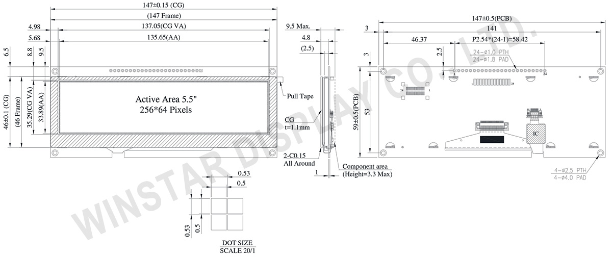
This module includes an integrated PCB that simplifies system integration by allowing direct wire connection without additional carrier board design. Multiple connection options such as PIN, FFC, CN, and FPC are supported. Four mounting holes are provided for easier mechanical installation.
The operating temperature range is -20°C to +70°C, and the storage temperature range is -30°C to +80°C.
This 5.5-inch OLED module is suitable for applications such as POS systems, vending machines, medical devices, and industrial control systems.
DRAWING
Data source ref:WEN025664DGPP3D00000
SPECIFICATIONS
General Specification
Item
Dimension
Unit
Dot Matrix
256 × 64 Dots
-
Module dimension
147.0 × 59 × 4.8
mm
Active Area
135.65 × 33.89
mm
Pixel Size
0.5 × 0.5
mm
Pixel Pitch
0.53 × 0.53
mm
Display Mode
Passive Matrix
Display Color
Monochrome
Drive Duty
1/64 Duty
Gray Scale
4 bits
OLED IC
SSD1322
OLED Interface
6800, 8080, SPI
Size
5.5 inch
CTP IC
GT911
Detect Point
1
CTP Interface
I2C
Surface
Normal Glare
Absolute Maximum Ratings
Parameter
Symbol
Min
Max
Unit
Supply Voltage for Display
VDD
-0.3
4
V
Operating Temperature
TOP
-20
+70
°C
Storage Temperature
TSTG
-30
+80
°C
Electronical Characteristics
DC Electrical Characteristics
Item
Symbol
Condition
Min
Typ
Max
Unit
Supply Voltage for Logic
VDD
-
2.8
3.0
3.3
V
High Level Input
VIH
-
0.8×VDD
-
VDD
V
Low Level Input
VIL
-
0
-
0.2×VDD
V
High Level Output
VOH
-
0.9×VDD
-
VDD
V
Low Level Output
VOL
-
0
-
0.1×VDD
V
50% Check Board operating Current
IDD
VDD =3V
-
240
400
mA
Interface Pin Function
Pin Number
Symbol
I/O
Function
1
VSS
P
Ground.
2
VDD
P
Power Supply for Core Logic Circuit
Power supply pin for core logic operation. A capacitor is required to connect between this pin and VSS
3
N.C.
P
Reserved Pin
The N.C. pin between function pins are reserved for compatible and flexible design.
4
D/C#
I
Data/Command Control
This pin is Data/Command control pin connecting to the MCU.
When the pin is pulled HIGH, the content at D[7:0] will be interpreted as data.
When the pin is pulled LOW, the content at D[7:0] will be interpreted as command.
5
R/W#
(WR#)
I
Read/Write Select or Write
This pin is MCU interface input. When interfacing to a 68XX-series microprocessor, this pin will be used as Read/Write (R/W#) selection input. Pull this pin to “High” for read mode and pull it to “Low” for write mode.
When 80XX interface mode is selected, this pin will be the Write (WR#) input. Data write operation is initiated when this pin is pulled low and the CS# is pulled low.
When serial mode is selected, this pin must be connected to VSS.
6
E/RD#
I
Read/Write Enable or Read
This pin is MCU interface input. When interfacing to a 68XX-series microprocessor, this pin will be used as the Enable (E) signal. Read/write operation is initiated when this pin is pulled high and the CS# is pulled low.
When connecting to an 80XX-microprocessor, this pin receives the Read (RD#) signal. Data read operation is initiated when this pin is pulled low and CS# is pulled low.
When serial mode is selected, this pin must be connected to VSS.
7~14
DB0
I/O
Host Data Input/Output Bus
These pins are 8-bit bi-directional data bus to be connected to the microprocessor’s data bus.
When serial mode is selected, D1 will be the serial data input SDIN and D0 will be the serial clock input SCLK.
DB1
DB2
DB3
DB4
DB5
DB6
DB7
15
NC
P
Reserved Pin
The N.C. pin between function pins are reserved for compatible and flexible design.
16
RES#
I
This pin is reset signal input.
When the pin is pulled LOW, initialization of the chip is executed.
Keep this pin pull HIGH during normal operation.
17
CS#
I
Data/Command Control
This pin is the chip select input connecting to the MCU. The chip is enabled for MCU communication only when CS# is pulled LOW.
18
NC
P
Reserved Pin
The N.C. pin between function pins are reserved for compatible and flexible design.
19
BS1
I
Communicating Protocol Select
These pins are MCU interface selection input. See the following table:
BS[1:0]
Bus Interface Selection
00
4 line SPI
01
3 line SPI
10
8-bit 8080 parallel
11
8-bit 6800 parallel
Note
(1) 0 is connected to VSS
(2) 1 is connected to VDD
By clicking "Allow All Cookies", you agree to the storing of cookies on your device to enhance site navigation, analyse site usage, and assist in our marketing and performance efforts. You can find further information this subject in our policy.
 - WEN025664D-CTP")
 - WEN025664D-CTP")
 - WEN025664D-CTP")
 - WEN025664D-CTP")
 - WEX025664D")
 - WEN025664D")
