WEN025664D-CTP è un modulo display OLED COF da 5,5” con PCB, cornice e touch capacitivo integrati. Presenta una risoluzione di 256x64 ed è pilotato dal controller SSD1322. Supporta interfacce 6800/8080 a 8 bit e SPI a 3/4 linee, funziona a 3V, utilizza un duty cycle 1/64 e offre scala di grigi a 4 bit.
Il pannello touch capacitivo (CTP) è basato su controller GT911 con interfaccia I2C, supporta il tocco singolo ed è dotato di vetro con finitura standard lucida, adatto per interfacce utente in sistemi embedded.
Il modulo integra una PCB che consente il collegamento diretto tramite cavi, riducendo la necessità di progettare schede aggiuntive. Supporta connessioni PIN, FFC, CN e FPC ed è dotato di quattro fori di fissaggio per una facile integrazione meccanica.
Temperatura operativa: -20°C ~ +70°C; temperatura di stoccaggio: -30°C ~ +80°C.
Adatto per POS, distributori automatici, dispositivi medicali e sistemi di controllo industriale.
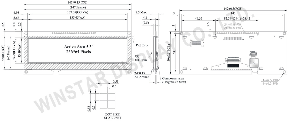
DISEGNO
Data source ref:WEN025664DGPP3D00000
SPECIFICHE TECNICHE
Specifiche generali
Caratteristica
Valore
Unità
Matrice di punti
256 × 64 Dots
-
Dimensioni del modulo
147.0 × 59 × 4.8
mm
Area attiva
135.65 × 33.89
mm
Dimensione pixel
0.5 × 0.5
mm
Passo pixel
0.53 × 0.53
mm
Modalità di visualizzazione
Matrice passiva
Colore del display
monocromatici
Duty di pilotaggio
1/64
Scala di grigi
4 bit
OLED IC
SSD1322
Interfaccia OLED
6800, 8080, SPI
Dimensione (diagonale)
5.5 inch
CTP IC
GT911
Punti di rilevamento
1
Interfaccia CTP
I2C
Superficie
Bagliore (Glare)
Valori massimi assoluti
Parametro
Simbolo
Min
Max
Unità
Tensione di alimentazione del display
VDD
-0.3
4
V
Temperatura di esercizio
TOP
-20
+70
°C
Temperatura di stoccaggio
TSTG
-30
+80
°C
Caratteristiche elettriche
Caratteristiche elettriche DC
Parametro
Simbolo
Condizioni
Min
Typ
Max
Unità
Tensione di alimentazione logica
VDD
-
2.8
3.0
3.3
V
Livello di ingresso alto
VIH
-
0.8×VDD
-
VDD
V
Livello di ingresso basso
VIL
-
0
-
0.2×VDD
V
Livello di uscita alto
VOH
-
0.9×VDD
-
VDD
V
Livello di uscita basso
VOL
-
0
-
0.1×VDD
V
Corrente operativa della scheda al 50%
IDD
VDD = 3V
-
240
400
mA
Funzione dei Pin di Interfaccia
Pin Number
Simbolo
I/O
Funzione
1
VSS
P
Ground.
2
VDD
P
Power Supply for Core Logic Circuit
Power supply pin for core logic operation. A capacitor is required to connect between this pin and VSS
3
N.C.
P
Reserved Pin
The N.C. pin between function pins are reserved for compatible and flexible design.
4
D/C#
I
Data/Command Control
This pin is Data/Command control pin connecting to the MCU.
When the pin is pulled HIGH, the content at D[7:0] will be interpreted as data.
When the pin is pulled LOW, the content at D[7:0] will be interpreted as command.
5
R/W#
(WR#)
I
Read/Write Select or Write
This pin is MCU interface input. When interfacing to a 68XX-series microprocessor, this pin will be used as Read/Write (R/W#) selection input. Pull this pin to “High” for read mode and pull it to “Low” for write mode.
When 80XX interface mode is selected, this pin will be the Write (WR#) input. Data write operation is initiated when this pin is pulled low and the CS# is pulled low.
When serial mode is selected, this pin must be connected to VSS.
6
E/RD#
I
Read/Write Enable or Read
This pin is MCU interface input. When interfacing to a 68XX-series microprocessor, this pin will be used as the Enable (E) signal. Read/write operation is initiated when this pin is pulled high and the CS# is pulled low.
When connecting to an 80XX-microprocessor, this pin receives the Read (RD#) signal. Data read operation is initiated when this pin is pulled low and CS# is pulled low.
When serial mode is selected, this pin must be connected to VSS.
7~14
DB0
I/O
Host Data Input/Output Bus
These pins are 8-bit bi-directional data bus to be connected to the microprocessor’s data bus.
When serial mode is selected, D1 will be the serial data input SDIN and D0 will be the serial clock input SCLK.
DB1
DB2
DB3
DB4
DB5
DB6
DB7
15
NC
P
Reserved Pin
The N.C. pin between function pins are reserved for compatible and flexible design.
16
RES#
I
This pin is reset signal input.
When the pin is pulled LOW, initialization of the chip is executed.
Keep this pin pull HIGH during normal operation.
17
CS#
I
Data/Command Control
This pin is the chip select input connecting to the MCU. The chip is enabled for MCU communication only when CS# is pulled LOW.
18
NC
P
Reserved Pin
The N.C. pin between function pins are reserved for compatible and flexible design.
19
BS1
I
Communicating Protocol Select
These pins are MCU interface selection input. See the following table:
BS[1:0]
Bus Interface Selection
00
4 line SPI
01
3 line SPI
10
8-bit 8080 parallel
11
8-bit 6800 parallel
Note
(1) 0 is connected to VSS
(2) 1 is connected to VDD
Facendo clic su "Consenti tutti i cookie", accetti la memorizzazione dei cookie sul tuo dispositivo per migliorare la navigazione del sito, analizzare l'utilizzo del sito e assistere nei nostri sforzi di marketing e prestazioni. Puoi trovare ulteriori informazioni su questo argomento nella nostra politica. Informativa sulla privacy