 - WEX025664D")
 - WEN025664D")
 I2Cインターフェース - SSD1315 IC | WEA012864V")
私たちはあなたのプライバシーを大切にします
「すべてのクッキーを許可」をクリックすると、サイトのナビゲーションを向上させ、サイト使用状況を分析し、マーケティングおよびパフォーマンスの取り組みを支援するために、クッキーをデバイスに保存することに同意したことになります。この件に関する詳細情報は、ポリシーをご覧ください。プライバシーポリシー

 - WEN025664D-CTP")
 - WEN025664D-CTP")
 - WEN025664D-CTP")
 - WEN025664D-CTP")
型番 WEN025664D-CTP
►タイプ: グラフィック有機ELモジュール
►結構: COF+FR+PCB
►サイズ: 5.5インチ
►256×64 ドットマトリックス
►IC:SSD1322
►3V電源電圧
►1/64 duty cycle
►インターフェース: 6800, 8080, SPI
►静電容量式タッチパネル(CTP)
►検出ポイント: 1
►発光色: 白色 / 黄色 / 緑色
►グレースケール機能をサポートする
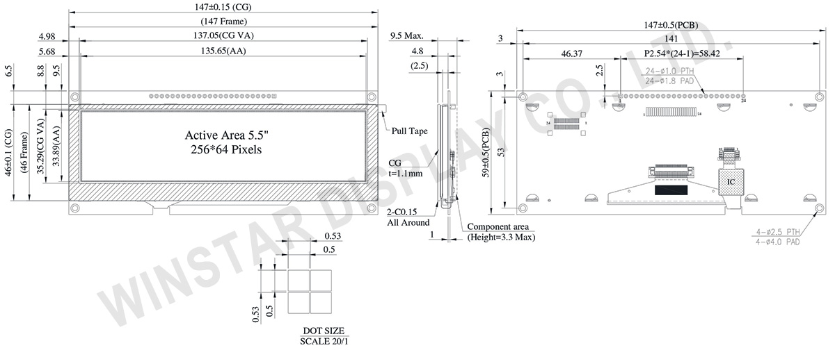
WEN025664D-CTPは、PCB・フレーム・静電容量式タッチパネルを一体化した5.5インチCOF OLEDディスプレイモジュールです。解像度は256×64、SSD1322コントローラICを搭載しています。6800/8080 8-bitパラレルおよび3/4線SPIに対応し、3V動作、1/64デューティ駆動、4-bitグレースケール表示に対応しています。
静電容量式タッチパネル(CTP)はGT911コントローラを採用し、I2Cインターフェースおよびシングルタッチ入力に対応しています。標準的なグレアガラスを採用しており、組込み機器のユーザーインターフェース用途に適しています。
本モジュールはPCBを統合しており、追加のキャリア基板設計なしでケーブル接続が可能です。PIN、FFC、CN、FPCなど複数の接続方式に対応し、基板上には4つの取付穴を備えています。
動作温度範囲:-20°C~+70°C、保存温度範囲:-30°C~+80°C。
その他のOLEDオプション:
POS端末、自動販売機、医療機器、産業機器などの用途に適しています。
| 項目 | 仕様 | 単位 |
|---|---|---|
| ドットマトリックス | 256 × 64 Dots | - |
| モジュールサイズ | 147.0 × 59 × 4.8 | mm |
| アクティブエリア | 135.65 × 33.89 | mm |
| ドットサイズ | 0.5 × 0.5 | mm |
| ドットピッチ | 0.53 × 0.53 | mm |
| 表示モード | パッシブマトリクス | |
| 発光色 | モノクロ | |
| 駆動方法 | 1/64 Duty | |
| グレースケール | 4 bits | |
| OLED IC | SSD1322 | |
| OLED インターフェイス | 6800, 8080, SPI | |
| 表示サイズ(対角線) | 5.5 インチ | |
| CTP IC | GT911 |
| 検出ポイント | 1 |
| CTP インターフェイス | I2C |
| 表面処理 | グレア |
| パラメーター | 記号 | 最小値 | 最大値 | 単位 |
|---|---|---|---|---|
| ディスプレイの供給電圧 | VDD | -0.3 | 4 | V |
| 操作温度 | TOP | -20 | +70 | °C |
| 保存温度 | TSTG | -30 | +80 | °C |
| 項目 | 記号 | 条件 | 最小値 | 典型値 | 最大値 | 単位 |
|---|---|---|---|---|---|---|
| ロジック電源電圧 | VDD | - | 2.8 | 3.0 | 3.3 | V |
| 高レベル入力 | VIH | - | 0.8×VDD | - | VDD | V |
| 低レベル入力 | VIL | - | 0 | - | 0.2×VDD | V |
| 高レベル出力 | VOH | - | 0.9×VDD | - | VDD | V |
| 低レベル出力 | VOL | - | 0 | - | 0.1×VDD | V |
| 50% チェックボード動作電流 | IDD | VDD =3V | - | 240 | 400 | mA |
| Pin Number | 記号 | I/O | 説明 | ||||||||||
|---|---|---|---|---|---|---|---|---|---|---|---|---|---|
| 1 | VSS | P | Ground. | ||||||||||
| 2 | VDD | P | Power Supply for Core Logic Circuit Power supply pin for core logic operation. A capacitor is required to connect between this pin and VSS |
||||||||||
| 3 | N.C. | P | Reserved Pin The N.C. pin between function pins are reserved for compatible and flexible design. |
||||||||||
| 4 | D/C# | I | Data/Command Control This pin is Data/Command control pin connecting to the MCU. When the pin is pulled HIGH, the content at D[7:0] will be interpreted as data. When the pin is pulled LOW, the content at D[7:0] will be interpreted as command. |
||||||||||
| 5 | R/W# (WR#) |
I | Read/Write Select or Write This pin is MCU interface input. When interfacing to a 68XX-series microprocessor, this pin will be used as Read/Write (R/W#) selection input. Pull this pin to “High” for read mode and pull it to “Low” for write mode. When 80XX interface mode is selected, this pin will be the Write (WR#) input. Data write operation is initiated when this pin is pulled low and the CS# is pulled low. When serial mode is selected, this pin must be connected to VSS. |
||||||||||
| 6 | E/RD# | I | Read/Write Enable or Read This pin is MCU interface input. When interfacing to a 68XX-series microprocessor, this pin will be used as the Enable (E) signal. Read/write operation is initiated when this pin is pulled high and the CS# is pulled low. When connecting to an 80XX-microprocessor, this pin receives the Read (RD#) signal. Data read operation is initiated when this pin is pulled low and CS# is pulled low. When serial mode is selected, this pin must be connected to VSS. |
||||||||||
| 7~14 | DB0 | I/O | Host Data Input/Output Bus These pins are 8-bit bi-directional data bus to be connected to the microprocessor’s data bus. When serial mode is selected, D1 will be the serial data input SDIN and D0 will be the serial clock input SCLK. |
||||||||||
| DB1 | |||||||||||||
| DB2 | |||||||||||||
| DB3 | |||||||||||||
| DB4 | |||||||||||||
| DB5 | |||||||||||||
| DB6 | |||||||||||||
| DB7 | |||||||||||||
| 15 | NC | P | Reserved Pin The N.C. pin between function pins are reserved for compatible and flexible design. |
||||||||||
| 16 | RES# | I | This pin is reset signal input. When the pin is pulled LOW, initialization of the chip is executed. Keep this pin pull HIGH during normal operation. |
||||||||||
| 17 | CS# | I | Data/Command Control This pin is the chip select input connecting to the MCU. The chip is enabled for MCU communication only when CS# is pulled LOW. |
||||||||||
| 18 | NC | P | Reserved Pin The N.C. pin between function pins are reserved for compatible and flexible design. |
||||||||||
| 19 | BS1 | I | Communicating Protocol Select These pins are MCU interface selection input. See the following table:
(1) 0 is connected to VSS (2) 1 is connected to VDD |
||||||||||
| 20 | BS0 | ||||||||||||
| 21 | TP_SCK | I | I2C clock input | ||||||||||
| 22 | TP_SDA | I | I2C data input and output | ||||||||||
| 23 | TP_INT | I | External interrupt to the host | ||||||||||
| 24 | TP_RST | I | External Reset, Low is active |

「すべてのクッキーを許可」をクリックすると、サイトのナビゲーションを向上させ、サイト使用状況を分析し、マーケティングおよびパフォーマンスの取り組みを支援するために、クッキーをデバイスに保存することに同意したことになります。この件に関する詳細情報は、ポリシーをご覧ください。プライバシーポリシー