 - WEN025664D-CTP")
 - WEX025664D")
私たちはあなたのプライバシーを大切にします
「すべてのクッキーを許可」をクリックすると、サイトのナビゲーションを向上させ、サイト使用状況を分析し、マーケティングおよびパフォーマンスの取り組みを支援するために、クッキーをデバイスに保存することに同意したことになります。この件に関する詳細情報は、ポリシーをご覧ください。プライバシーポリシー

 - WEN025664D")
 - WEN025664D")
 - WEN025664D")
 - WEN025664D")
 - WEN025664D")
 - WEN025664D")
 - WEN025664D")
型番 WEN025664D
►タイプ: グラフィック有機EL液晶
►結構: COF+Frame+PCB
►サイズ: 5.5インチ
►256 x 64 Dot Matrix
►IC:SSD1322
►3V電源電圧
►1/64 duty
►インターフェース: 6800, 8080, SPI
►発光色: 白色 / 黄色 / 緑色
►グレースケール機能をサポートする
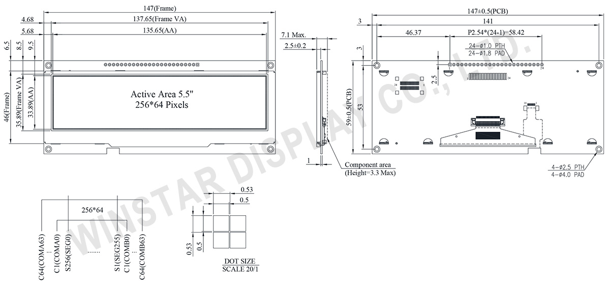
WEN025664Dは、SSD1322コントローラICを内蔵した5.5インチのCOF OLEDディスプレイモジュールです。解像度は256×64ドット、モジュール外形寸法は135.65 × 33.89 mmです。6800/8080 8-bitパラレルインターフェースおよび3/4線SPIに対応し、3V電源で動作します。1/64デューティ駆動方式を採用し、4-bitグレースケール表示および10000:1のコントラスト比を備えています。
本モジュールはフレーム付きPCB基板を搭載しており、ケーブル接続によるシステム実装が可能です。追加のキャリア基板設計を削減でき、PCBにはインターフェース設定およびVDD回路が統合されているため、システム統合が容易です。また、基板上には4箇所の取付穴があり、機器への組み込みがしやすい構造となっています。
動作温度範囲は-40℃~+80℃、保存温度範囲は-40℃~+85℃で、広温度範囲が求められる用途に対応します。
その他のOLEDパネルオプション:
本5.5インチOLEDモジュールは、POS端末、自動販売機、携帯機器、医療機器、産業機器などの用途に適しています。
| 項目 | 仕様 | 単位 |
|---|---|---|
| ドットマトリックス | 256 × 64 Dots | - |
| モジュールサイズ | 147.0 × 59 × 2.5 | mm |
| アクティブエリア | 135.65 × 33.89 | mm |
| ピクセルサイズ | 0.50 × 0.50 | mm |
| ピクセルピッチ | 0.53 × 0.53 | mm |
| 表示モード | パッシブマトリクス | |
| 発光色 | モノクロ | |
| 駆動方法 | 1/64 Duty | |
| グレースケール | 4 bits | |
| IC | SSD1322 | |
| インターフェイス | 6800, 8080, SPI | |
| サイズ | 5.5 インチ | |
| パラメーター | 記号 | 最小値 | 最大値 | 単位 |
|---|---|---|---|---|
| ディスプレイの供給電圧 | VDD | -0.3 | 4 | V |
| 操作温度 | TOP | -40 | +80 | °C |
| 保存温度 | TSTG | -40 | +85 | °C |
| 項目 | 記号 | 条件 | 最小値 | 典型値 | 最大値 | 単位 |
|---|---|---|---|---|---|---|
| ロジック電源電圧 | VDD | - | 2.8 | 3.0 | 3.3 | V |
| 高レベル入力 | VIH | - | 0.8×VDD | - | VDD | V |
| 低レベル入力 | VIL | - | 0 | - | 0.2×VDD | V |
| 高レベル出力 | VOH | - | 0.9×VDD | - | VDD | V |
| 低レベル出力 | VOL | - | 0 | - | 0.1×VDD | V |
| ディスプレイ50%ピクセル点灯 | IDD | VDD =3V | - | 240 | 400 | mA |
| Pin Number |
記号 | I/O | 説明 | ||||||||||
|---|---|---|---|---|---|---|---|---|---|---|---|---|---|
| 1 | VSS | P | Ground. | ||||||||||
| 2 | VDD | P | Power Supply for Core Logic Circuit Power supply pin for core logic operation. A capacitor is required to connect between this pin and VSS |
||||||||||
| 3 | N.C. | P | Reserved Pin The N.C. pin between function pins are reserved for compatible and flexible design. |
||||||||||
| 4 | D/C# | I | Data/Command Control This pin is Data/Command control pin connecting to the MCU. When the pin is pulled HIGH, the content at D[7:0] will be interpreted as data. When the pin is pulled LOW, the content at D[7:0] will be interpreted as command. |
||||||||||
| 5 | R/W# (WR#) |
I | Read/Write Select or Write This pin is MCU interface input. When interfacing to a 68XX-series microprocessor, this pin will be used as Read/Write (R/W#) selection input. Pull this pin to “High” for read mode and pull it to “Low” for write mode. When 80XX interface mode is selected, this pin will be the Write (WR#) input. Data write operation is initiated when this pin is pulled low and the CS# is pulled low. When serial mode is selected, this pin must be connected to VSS. |
||||||||||
| 6 | E(/RD#) | I | Read/Write Enable or Read This pin is MCU interface input. When interfacing to a 68XX-series microprocessor, this pin will be used as the Enable (E) signal. Read/write operation is initiated when this pin is pulled high and the CS# is pulled low. When connecting to an 80XX-microprocessor, this pin receives the Read (RD#) signal. Data read operation is initiated when this pin is pulled low and CS# is pulled low. When serial mode is selected, this pin must be connected to VSS. |
||||||||||
| 7~14 | DB0 | I/O | Host Data Input/Output Bus These pins are 8-bit bi-directional data bus to be connected to the microprocessor’s data bus. When serial mode is selected, D1 will be the serial data input SDIN and D0 will be the serial clock input SCLK. |
||||||||||
| DB1 | |||||||||||||
| DB2 | |||||||||||||
| DB3 | |||||||||||||
| DB4 | |||||||||||||
| DB5 | |||||||||||||
| DB6 | |||||||||||||
| DB7 | |||||||||||||
| 15 | NC | P | Reserved Pin The N.C. pin between function pins are reserved for compatible and flexible design. |
||||||||||
| 16 | RES# | I | This pin is reset signal input. When the pin is pulled LOW, initialization of the chip is executed. Keep this pin pull HIGH during normal operation. |
||||||||||
| 17 | CS# | I | Data/Command Control This pin is the chip select input connecting to the MCU. The chip is enabled for MCU communication only when CS# is pulled LOW. |
||||||||||
| 18 | NC | P | Reserved Pin The N.C. pin between function pins are reserved for compatible and flexible design. |
||||||||||
| 19 | BS1 | I | Communicating Protocol Select These pins are MCU interface selection input. See the following table:
(1) 0 is connected to VSS (2) 1 is connected to VDD |
||||||||||
| 20 | BS0 | ||||||||||||
| 21 | NC | - | No connection | ||||||||||
| 22 | NC | - | No connection | ||||||||||
| 23 | NC | - | No connection | ||||||||||
| 24 | NC | - | No connection |

「すべてのクッキーを許可」をクリックすると、サイトのナビゲーションを向上させ、サイト使用状況を分析し、マーケティングおよびパフォーマンスの取り組みを支援するために、クッキーをデバイスに保存することに同意したことになります。この件に関する詳細情報は、ポリシーをご覧ください。プライバシーポリシー