 - WEN025664D-CTP")
 - WEN025664D")
私たちはあなたのプライバシーを大切にします
「すべてのクッキーを許可」をクリックすると、サイトのナビゲーションを向上させ、サイト使用状況を分析し、マーケティングおよびパフォーマンスの取り組みを支援するために、クッキーをデバイスに保存することに同意したことになります。この件に関する詳細情報は、ポリシーをご覧ください。プライバシーポリシー

 - WEX025664D")
 - WEX025664D")
 - WEX025664D")
 - WEX025664D")
 - WEX025664D")
 - WEX025664D")
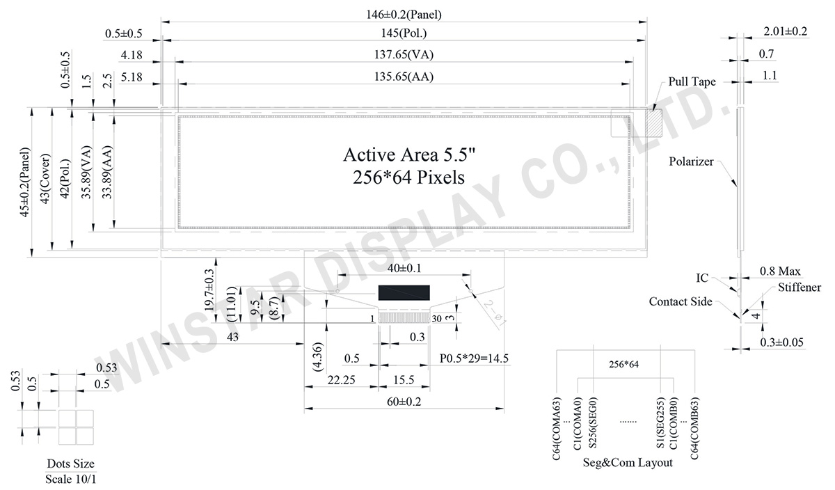
WEX025664Dは、5.5インチのCOF OLEDディスプレイモジュールで、解像度は256×64ドットです。SSD1322ドライバICを内蔵し、6800 / 8080 8ビットパラレルインターフェースおよび3-/4ラインSPIインターフェースに対応しており、システム設計における柔軟な接続が可能です。
動作電圧は3V、1/64デューティ駆動方式を採用し、4ビットグレースケールに対応しています。コントラスト比は10,000:1で、安定した表示性能を提供します。動作温度範囲は-40℃~+80℃、保存温度範囲は-40℃~+85℃で、さまざまな環境での使用に適しています。
WEX025664DはCOF(Chip on Film)構造を採用した有機ELディスプレイで、自己発光方式のためバックライトを必要とせず、薄型・軽量・低消費電力設計に適しています。
本モジュールは、計測機器、ホームオートメーション機器、POSシステム、IoT機器、ハンディ機器、車載ディスプレイ、通信機器、医療機器などの用途に適しています。
同シリーズには以下のオプションも用意されています:
| 項目 | 仕様 | 単位 |
|---|---|---|
| モジュールサイズ | 256 x 64 Dots | - |
| 表示エリア | 146.0 × 45.0 × 2.01 | mm |
| アクティブエリア | 135.65 × 33.89 | mm |
| ドットサイズ | 0.50 × 0.50 | mm |
| ドットピッチ | 0.53 × 0.53 | mm |
| 表示モード | パッシブマトリクス | |
| 表示カラー | モノクロ | |
| 駆動方法 | 1/64 Duty | |
| グレースケール | 4 bits | |
| IC | SSD1322 | |
| インターフェイス | 6800, 8080, SPI | |
| サイズ | 5.5 インチ | |
| パラメーター | 記号 | 最小値 | 最大値 | 単位 |
|---|---|---|---|---|
| ロジック電源電圧 | VDD | -0.5 | 2.75 | V |
| 低電圧電源 | VCI | -0.3 | 4.0 | V |
| 入力/出力ピンの電源電圧 | VDDIO | -0.5 | VCI | V |
| 表示用電源電圧 | VCC | -0.5 | 21.0 | V |
| 操作温度 | TOP | -40 | +80 | °C |
| 保存温度 | TSTG | -40 | +85 | °C |
| 項目 | 記号 | 条件 | 最小値 | 典型値 | 最大値 | 単位 |
|---|---|---|---|---|---|---|
| ロジック電源電圧 | VDD | - | 2.4 | 2.5 | 2.6 | V |
| 入力/出力ピンの電源電圧 | VDDIO | - | 1.65 | 3.0 | VCI | V |
| 低電圧電源 | VCI | - | 2.4 | 3.0 | 3.5 | V |
| 表示用電源電圧 | VCC | - | 10.0 | 18.0 | 18.5 | V |
| 高レベル入力 | VIH | - | 0.8×VDDIO | - | VDDIO | V |
| 低レベル入力 | VIL | - | 0 | - | 0.2×VDDIO | V |
| 高レベル出力 | VOH | - | 0.9×VDDIO | - | VDDIO | V |
| 低レベル出力 | VOL | - | 0 | - | 0.1×VDDIO | V |
| ディスプレイ30%ピクセル点灯 | ICC | VCC =18V | - | 40 | 60 | mA |
| No. | 記号 | 説明 | ||||||||||
|---|---|---|---|---|---|---|---|---|---|---|---|---|
| 1 | N.C. | The N.C. pin between function pins are reserved for compatible and flexible design. | ||||||||||
| 2 | VSS | Ground. | ||||||||||
| 3 | VCC | Power supply for panel driving voltage. This is also the most positive power voltage supply pin. |
||||||||||
| 4 | VCOMH | COM signal deselected voltage level. A capacitor should be connected between this pin and VSS. |
||||||||||
| 5 | VLSS | Analog system ground pin. | ||||||||||
| 6~13 | D7~D0 | These pins are bi-directional data bus connecting to the MCU data bus. Unused pins are recommended to tie LOW. (Except for D2 pin in SPI mode) |
||||||||||
| 14 | E/RD# | This pin is MCU interface input. When interfacing to a 6800-series microprocessor, this pin will be used as the Enable (E) signal. Read/write operation is initiated when this pin is pulled HIGH and the chip is selected. When connecting to an 8080-microprocessor, this pin receives the Read (RD#) signal. Read operation is initiated when this pin is pulled LOW and the chip is selected. When serial interface is selected, this pin E(RD#) must be connected to VSS. |
||||||||||
| 15 | R/W# | This pin is read / write control input pin connecting to the MCU interface. When interfacing to a 6800-series microprocessor, this pin will be used as Read/Write (R/W#) selection input. Read mode will be carried out when this pin is pulled HIGH and write mode when LOW. When 8080 interface mode is selected, this pin will be the Write (WR#) input. Data write operation is initiated when this pin is pulled LOW and the chip is selected. When serial interface is selected, this pin R/W (WR#) must be connected to VSS. |
||||||||||
| 16 | BS0 | MCU bus interface selection pins. Select appropriate logic setting as described in the following table.
(1) 0 is connected to VSS (2) 1 is connected to VDDIO |
||||||||||
| 17 | BS1 | |||||||||||
| 18 | D/C# | This pin is Data/Command control pin connecting to the MCU. When the pin is pulled HIGH, the content at D[7:0] will be interpreted as data. When the pin is pulled LOW, the content at D[7:0] will be interpreted as command. |
||||||||||
| 19 | CS# | This pin is the chip select input connecting to the MCU. The chip is enabled for MCU communication only when CS# is pulled LOW. | ||||||||||
| 20 | RES# | This pin is reset signal input. When the pin is pulled LOW, initialization of the chip is executed. Keep this pin pull HIGH during normal operation. |
||||||||||
| 21 | FR | This pin is No Connection pins. Nothing should be connected to this pin. This pin should be left open individually. | ||||||||||
| 22 | IREF | This pin is the segment output current reference pin. A resistor should be connected between this pin and VSS to maintain the current around 10uA. |
||||||||||
| 23 | N.C. | The N.C. pin between function pins are reserved for compatible and flexible design. | ||||||||||
| 24 | VDDIO | Power supply for interface logic level. It should be matched with the MCU interface voltage level. | ||||||||||
| 25 | VDD | Power supply pin for core logic operation. A capacitor is required to connect between this pin and VSS. | ||||||||||
| 26 | VCI | Low voltage power supply. VCI must always be equal to or higher than VDD and VDDIO. |
||||||||||
| 27 | VSL | This is segment voltage reference pin. When external VSL is used, connect with resistor and diode to ground. |
||||||||||
| 28 | VLSS | Analog system ground pin. | ||||||||||
| 29 | VCC | Power supply for panel driving voltage. This is also the most positive power voltage supply pin. |
||||||||||
| 30 | N.C. | The N.C. pin between function pins are reserved for compatible and flexible design. |

「すべてのクッキーを許可」をクリックすると、サイトのナビゲーションを向上させ、サイト使用状況を分析し、マーケティングおよびパフォーマンスの取り組みを支援するために、クッキーをデバイスに保存することに同意したことになります。この件に関する詳細情報は、ポリシーをご覧ください。プライバシーポリシー