 - WEN025664D-CTP")
 - WEN025664D")
我们重视您的隐私
通过点击「允许所有 Cookie」,代表您同意在您的设备上存储 Cookie 以增强网站浏览体验、分析网站使用情况并协助我们的营销和网站效能优化工作。您可以在我们的隐私权政策中找到有关于此的更多信息。
 - WEX025664D")
 - WEX025664D")
 - WEX025664D")
 - WEX025664D")
 - WEX025664D")
 - WEX025664D")
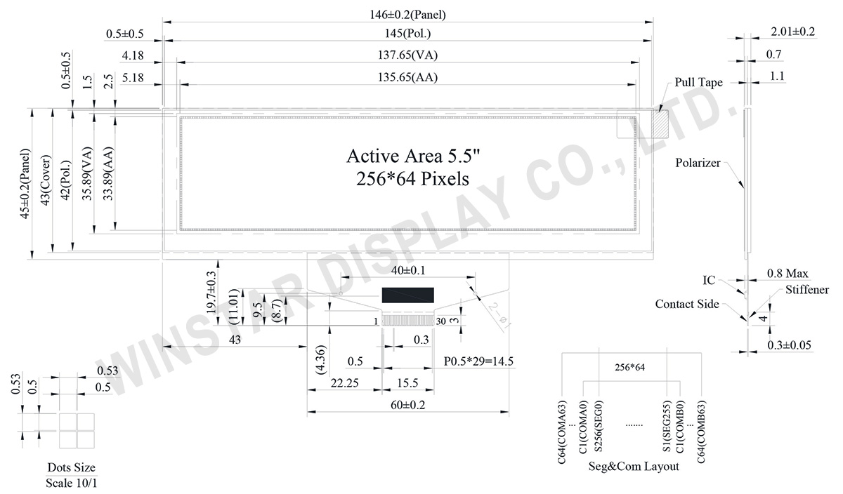
WEX025664D为5.5寸COF OLED显示模块,分辨率为256×64 dots。本模块内置SSD1322驱动IC,支持6800 / 8080 8-bit并行接口以及3-/4-line SPI接口,可提供灵活的系统集成方式。
模块工作电压为3V,采用1/64 duty驱动方式,支持4-bit灰阶,对比度达10000:1,可实现稳定且清晰的显示效果。工作温度范围为-40℃至+80℃,存储温度范围为-40℃至+85℃,适用于多种环境条件。
WEX025664D采用COF(Chip on Film)结构,属于自发光OLED显示技术,无需背光源,有助于实现轻薄化和低功耗设计。
该模块适用于测量仪表、家用自动化设备、POS系统、云端/物联网应用、手持设备、车载显示、通信设备及医疗设备等。
同系列产品还提供以下选项:
| 项目 | 尺寸 | 单位 |
|---|---|---|
| 点阵 | 256 x 64 Dots | - |
| 模块尺寸 | 146.0 × 45.0 × 2.01 | mm |
| 有效区域 | 135.65 × 33.89 | mm |
| 像素大小 | 0.50 × 0.50 | mm |
| 像素间距 | 0.53 × 0.53 | mm |
| 显示模块 | 被动矩阵 | |
| 显示颜色 | 单色 | |
| 驱动方式 | 1/64 Duty | |
| 灰阶 | 4 bits | |
| IC | SSD1322 | |
| 接口 | 6800, 8080, SPI | |
| 尺寸 | 5.5 寸 | |
| 参数 | 符号 | 最小值 | 最大值 | 单位 |
|---|---|---|---|---|
| 逻辑电源电压 | VDD | -0.5 | 2.75 | V |
| 低压电源 | VCI | -0.3 | 4.0 | V |
| 输入/输出Pin供电电压 | VDDIO | -0.5 | VCI | V |
| 显示电源电压 | VCC | -0.5 | 21.0 | V |
| 工作温度 | TOP | -40 | +80 | °C |
| 储存温度 | TSTG | -40 | +85 | °C |
| 项目 | 符号 | 条件 | 最小值 | 典型值 | 最大值 | 单位 |
|---|---|---|---|---|---|---|
| 逻辑电源电压 | VDD | - | 2.4 | 2.5 | 2.6 | V |
| 输入/输出Pin供电电压 | VDDIO | - | 1.65 | 3.0 | VCI | V |
| 低压电源 | VCI | - | 2.4 | 3.0 | 3.5 | V |
| 显示电源电压 | VCC | - | 10.0 | 18.0 | 18.5 | V |
| 输入高准位 | VIH | - | 0.8×VDDIO | - | VDDIO | V |
| 输入低准位 | VIL | - | 0 | - | 0.2×VDDIO | V |
| 输出高准位 | VOH | - | 0.9×VDDIO | - | VDDIO | V |
| 输出低准位 | VOL | - | 0 | - | 0.1×VDDIO | V |
| 显示屏 30% 像素开启 | ICC | VCC =18V | - | 40 | 60 | mA |
| No. | 符号 | 功能说明 | ||||||||||
|---|---|---|---|---|---|---|---|---|---|---|---|---|
| 1 | N.C. | The N.C. pin between function pins are reserved for compatible and flexible design. | ||||||||||
| 2 | VSS | Ground. | ||||||||||
| 3 | VCC | Power supply for panel driving voltage. This is also the most positive power voltage supply pin. |
||||||||||
| 4 | VCOMH | COM signal deselected voltage level. A capacitor should be connected between this pin and VSS. |
||||||||||
| 5 | VLSS | Analog system ground pin. | ||||||||||
| 6~13 | D7~D0 | These pins are bi-directional data bus connecting to the MCU data bus. Unused pins are recommended to tie LOW. (Except for D2 pin in SPI mode) |
||||||||||
| 14 | E/RD# | This pin is MCU interface input. When interfacing to a 6800-series microprocessor, this pin will be used as the Enable (E) signal. Read/write operation is initiated when this pin is pulled HIGH and the chip is selected. When connecting to an 8080-microprocessor, this pin receives the Read (RD#) signal. Read operation is initiated when this pin is pulled LOW and the chip is selected. When serial interface is selected, this pin E(RD#) must be connected to VSS. |
||||||||||
| 15 | R/W# | This pin is read / write control input pin connecting to the MCU interface. When interfacing to a 6800-series microprocessor, this pin will be used as Read/Write (R/W#) selection input. Read mode will be carried out when this pin is pulled HIGH and write mode when LOW. When 8080 interface mode is selected, this pin will be the Write (WR#) input. Data write operation is initiated when this pin is pulled LOW and the chip is selected. When serial interface is selected, this pin R/W (WR#) must be connected to VSS. |
||||||||||
| 16 | BS0 | MCU bus interface selection pins. Select appropriate logic setting as described in the following table.
(1) 0 is connected to VSS (2) 1 is connected to VDDIO |
||||||||||
| 17 | BS1 | |||||||||||
| 18 | D/C# | This pin is Data/Command control pin connecting to the MCU. When the pin is pulled HIGH, the content at D[7:0] will be interpreted as data. When the pin is pulled LOW, the content at D[7:0] will be interpreted as command. |
||||||||||
| 19 | CS# | This pin is the chip select input connecting to the MCU. The chip is enabled for MCU communication only when CS# is pulled LOW. | ||||||||||
| 20 | RES# | This pin is reset signal input. When the pin is pulled LOW, initialization of the chip is executed. Keep this pin pull HIGH during normal operation. |
||||||||||
| 21 | FR | This pin is No Connection pins. Nothing should be connected to this pin. This pin should be left open individually. | ||||||||||
| 22 | IREF | This pin is the segment output current reference pin. A resistor should be connected between this pin and VSS to maintain the current around 10uA. |
||||||||||
| 23 | N.C. | The N.C. pin between function pins are reserved for compatible and flexible design. | ||||||||||
| 24 | VDDIO | Power supply for interface logic level. It should be matched with the MCU interface voltage level. | ||||||||||
| 25 | VDD | Power supply pin for core logic operation. A capacitor is required to connect between this pin and VSS. | ||||||||||
| 26 | VCI | Low voltage power supply. VCI must always be equal to or higher than VDD and VDDIO. |
||||||||||
| 27 | VSL | This is segment voltage reference pin. When external VSL is used, connect with resistor and diode to ground. |
||||||||||
| 28 | VLSS | Analog system ground pin. | ||||||||||
| 29 | VCC | Power supply for panel driving voltage. This is also the most positive power voltage supply pin. |
||||||||||
| 30 | N.C. | The N.C. pin between function pins are reserved for compatible and flexible design. |

通过点击「允许所有 Cookie」,代表您同意在您的设备上存储 Cookie 以增强网站浏览体验、分析网站使用情况并协助我们的营销和网站效能优化工作。您可以在我们的隐私权政策中找到有关于此的更多信息。