 - WEN025664D-CTP")
 - WEN025664D")
我們重視您的隱私
通過點擊「允許所有 Cookie」,代表您同意在您的設備上存儲 Cookie 以增強網站瀏覽體驗、分析網站使用情況並協助我們的行銷和網站效能優化工作。您可以在我們的隱私權政策中找到有關於此的更多資訊。

 - WEX025664D")
 - WEX025664D")
 - WEX025664D")
 - WEX025664D")
 - WEX025664D")
 - WEX025664D")
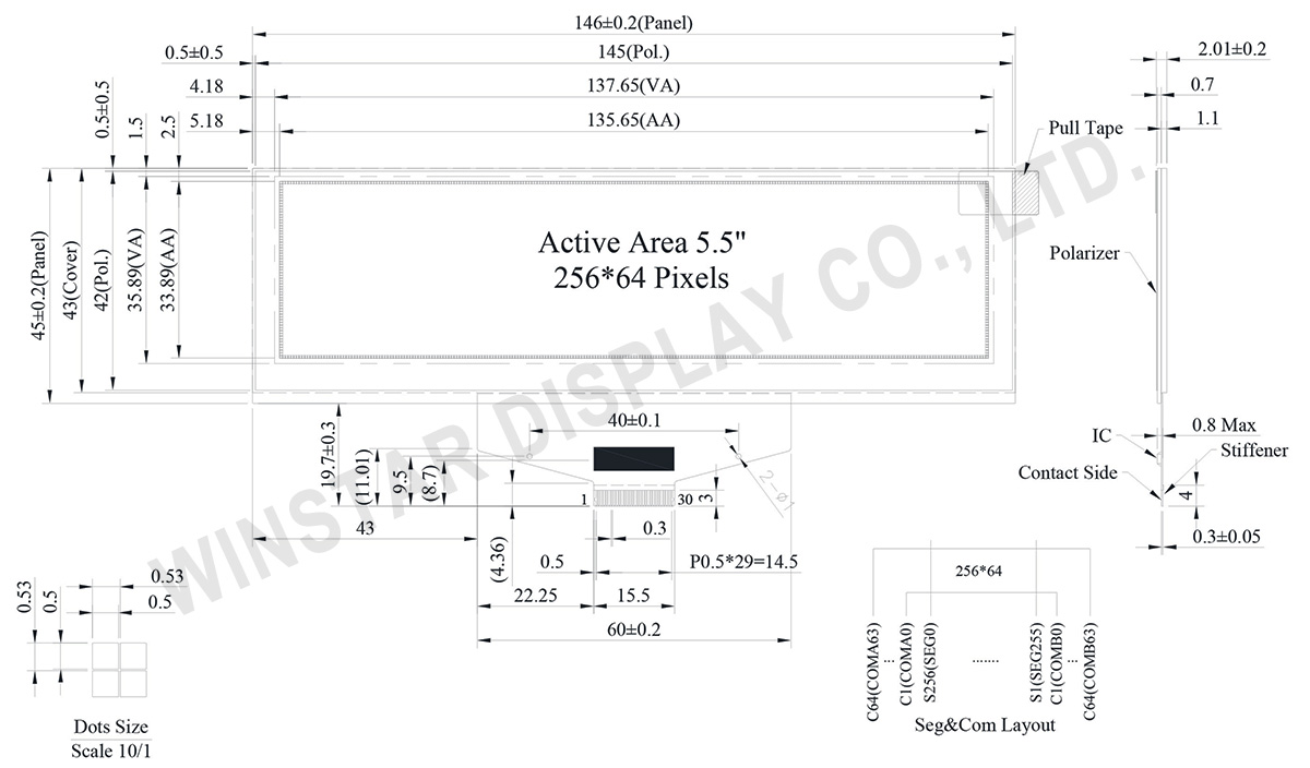
WEX025664D為5.5吋COF OLED顯示模組,解析度為256×64 dots。模組內建SSD1322驅動IC,支援6800 / 8080 8-bit並列介面與3-/4-line SPI介面,可提供彈性的系統整合方式。
模組工作電壓為3V,採用1/64 duty驅動方式,支援4-bit灰階,對比度達10000:1,可呈現穩定且清晰的顯示效果。工作溫度範圍為-40℃至+80℃,儲存溫度範圍為-40℃至+85℃,適用於多種環境條件。
WEX025664D採用COF(Chip on Film)結構,為自發光OLED顯示技術,無需背光源,有助於實現輕薄與低功耗設計。
此模組適用於測量儀器、家用自動化設備、POS系統、雲端/物聯網應用、手持式裝置、車載顯示、通訊設備及醫療儀器等。
同系列產品亦提供以下選項:
| 項目 | 尺寸 | 單位 |
|---|---|---|
| 點陣 | 256 x 64 Dots | - |
| 模組尺寸 | 146.0 × 45.0 × 2.01 | mm |
| 有效區域 | 135.65 × 33.89 | mm |
| 像素大小 | 0.50 × 0.50 | mm |
| 像素間距 | 0.53 × 0.53 | mm |
| 顯示模組 | 被動矩陣 | |
| 顯示顏色 | 單色 | |
| 驅動方式 | 1/64 Duty | |
| 灰階 | 4 bits | |
| IC | SSD1322 | |
| 介面 | 6800, 8080, SPI | |
| 尺寸 | 5.5 吋 | |
| 參數 | 符號 | 最小值 | 最大值 | 單位 |
|---|---|---|---|---|
| 邏輯電源電壓 | VDD | -0.5 | 2.75 | V |
| 低壓電源 | VCI | -0.3 | 4.0 | V |
| 輸入/輸出Pin供電電壓 | VDDIO | -0.5 | VCI | V |
| 顯示電源電壓 | VCC | -0.5 | 21.0 | V |
| 工作溫度 | TOP | -40 | +80 | °C |
| 儲存溫度 | TSTG | -40 | +85 | °C |
| 項目 | 符號 | 條件 | 最小值 | 典型值 | 最大值 | 單位 |
|---|---|---|---|---|---|---|
| 邏輯電源電壓 | VDD | - | 2.4 | 2.5 | 2.6 | V |
| 輸入/輸出Pin供電電壓 | VDDIO | - | 1.65 | 3.0 | VCI | V |
| 低壓電源 | VCI | - | 2.4 | 3.0 | 3.5 | V |
| 顯示電源電壓 | VCC | - | 10.0 | 18.0 | 18.5 | V |
| 輸入高準位 | VIH | - | 0.8×VDDIO | - | VDDIO | V |
| 輸入低準位 | VIL | - | 0 | - | 0.2×VDDIO | V |
| 輸出高準位 | VOH | - | 0.9×VDDIO | - | VDDIO | V |
| 輸出低準位 | VOL | - | 0 | - | 0.1×VDDIO | V |
| 顯示器 30% 像素開啟 | ICC | VCC =18V | - | 40 | 60 | mA |
| No. | 符號 | 功能說明 | ||||||||||
|---|---|---|---|---|---|---|---|---|---|---|---|---|
| 1 | N.C. | The N.C. pin between function pins are reserved for compatible and flexible design. | ||||||||||
| 2 | VSS | Ground. | ||||||||||
| 3 | VCC | Power supply for panel driving voltage. This is also the most positive power voltage supply pin. |
||||||||||
| 4 | VCOMH | COM signal deselected voltage level. A capacitor should be connected between this pin and VSS. |
||||||||||
| 5 | VLSS | Analog system ground pin. | ||||||||||
| 6~13 | D7~D0 | These pins are bi-directional data bus connecting to the MCU data bus. Unused pins are recommended to tie LOW. (Except for D2 pin in SPI mode) |
||||||||||
| 14 | E/RD# | This pin is MCU interface input. When interfacing to a 6800-series microprocessor, this pin will be used as the Enable (E) signal. Read/write operation is initiated when this pin is pulled HIGH and the chip is selected. When connecting to an 8080-microprocessor, this pin receives the Read (RD#) signal. Read operation is initiated when this pin is pulled LOW and the chip is selected. When serial interface is selected, this pin E(RD#) must be connected to VSS. |
||||||||||
| 15 | R/W# | This pin is read / write control input pin connecting to the MCU interface. When interfacing to a 6800-series microprocessor, this pin will be used as Read/Write (R/W#) selection input. Read mode will be carried out when this pin is pulled HIGH and write mode when LOW. When 8080 interface mode is selected, this pin will be the Write (WR#) input. Data write operation is initiated when this pin is pulled LOW and the chip is selected. When serial interface is selected, this pin R/W (WR#) must be connected to VSS. |
||||||||||
| 16 | BS0 | MCU bus interface selection pins. Select appropriate logic setting as described in the following table.
(1) 0 is connected to VSS (2) 1 is connected to VDDIO |
||||||||||
| 17 | BS1 | |||||||||||
| 18 | D/C# | This pin is Data/Command control pin connecting to the MCU. When the pin is pulled HIGH, the content at D[7:0] will be interpreted as data. When the pin is pulled LOW, the content at D[7:0] will be interpreted as command. |
||||||||||
| 19 | CS# | This pin is the chip select input connecting to the MCU. The chip is enabled for MCU communication only when CS# is pulled LOW. | ||||||||||
| 20 | RES# | This pin is reset signal input. When the pin is pulled LOW, initialization of the chip is executed. Keep this pin pull HIGH during normal operation. |
||||||||||
| 21 | FR | This pin is No Connection pins. Nothing should be connected to this pin. This pin should be left open individually. | ||||||||||
| 22 | IREF | This pin is the segment output current reference pin. A resistor should be connected between this pin and VSS to maintain the current around 10uA. |
||||||||||
| 23 | N.C. | The N.C. pin between function pins are reserved for compatible and flexible design. | ||||||||||
| 24 | VDDIO | Power supply for interface logic level. It should be matched with the MCU interface voltage level. | ||||||||||
| 25 | VDD | Power supply pin for core logic operation. A capacitor is required to connect between this pin and VSS. | ||||||||||
| 26 | VCI | Low voltage power supply. VCI must always be equal to or higher than VDD and VDDIO. |
||||||||||
| 27 | VSL | This is segment voltage reference pin. When external VSL is used, connect with resistor and diode to ground. |
||||||||||
| 28 | VLSS | Analog system ground pin. | ||||||||||
| 29 | VCC | Power supply for panel driving voltage. This is also the most positive power voltage supply pin. |
||||||||||
| 30 | N.C. | The N.C. pin between function pins are reserved for compatible and flexible design. |

通過點擊「允許所有 Cookie」,代表您同意在您的設備上存儲 Cookie 以增強網站瀏覽體驗、分析網站使用情況並協助我們的行銷和網站效能優化工作。您可以在我們的隱私權政策中找到有關於此的更多資訊。