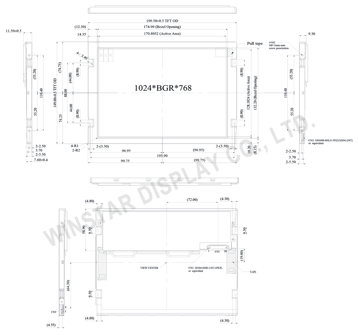
Wide Temperature 8.4" LVDS TFT LCD Display
Model No. WF0840ATWAMLNN0
►Size : 8.4”
►Resolution : 1024 x 768 dots
►View Direction : 80/80/80/80 (IPS)
►Interface : LVDS
►Driver IC : ST5821AH+ST5084AA
►Control-Board : No
►Brightness (cd/m²): 500
►Frame Through Hole : No
►Touch Screen : NO
►Operating Temperature : -30~+80 °C (Wide Temperature)
Description
WF0840ATWAMLNN0 is an 8.4-inch Wide Temperature IPS TFT-LCD module made of resolution 1024x768 pixels. This module is built-in with ST5821AH and ST5084AA driver ICs, and it supports LVDS interface. WF0840ATWAMLNN0 is adopted IPS panel which is having the advantage of wider view angle of Left:80 / Right:80 / Up:80 / Down:80 degree (typical), contrast ratio 1000:1 (typical value), brightness 500 nits (typical value), anti-glare surface panel, aspect ratio 4:3. If customers need a High Brightness version, please choose WF0840ASWAMLNN0.
The supply voltage (VDD) of WF0840ATWAMLNN0 is from 3.0V to 3.6V, the typical value of 3.3V. It can be operating at temperatures from -30℃ to+ 80℃ and storage temperatures from -30℃ to +80℃. WF0840A series has a projected capacitive touch panel module no. WF0840ATWAMLNB0 and WF0840ASWAMLNB0 (High Brightness version) for options.
Mitsubishi announced that it would end production of TFT-LCD modules manufacturing. Customers can choose our WF0840ATWAMLNN0 as a replacement for Mitsubishi 8.4” P/No. AA084XB01.
DRAWING
SPECIFICATIONS
Interface
LCM PIN Definition
Pin No. | Symbol | Function |
---|---|---|
1 | VDD | Power supply |
2 | VDD | Power supply |
3 | GND | Ground |
4 | GND | Ground |
5 | Link0- | 0- LVDS differential data input (D0N) |
6 | Link0+ | 0+ LVDS differential data input (D0P) |
7 | GND | Ground |
8 | Link1- | 1- LVDS differential data input (D1N) |
9 | Link1+ | 1+ LVDS differential data input (D1P) |
10 | GND | Ground |
11 | Link2- | 2- LVDS differential data input (D2N) |
12 | Link2+ | 2+ LVDS differential data input (D2P) |
13 | GND | Ground |
14 | CLKIN- | - LVDS differential clock input (CLKN) |
15 | CLKIN+ | + LVDS differential clock input (CLKP) |
16 | GND | Ground |
17 | Link3- | 3- LVDS differential data input (D3N) |
18 | Link3+ | 3+ LVDS differential data input (D3P) |
19 | MODE | Bit 6/8:Low(6 Bit);High(8 Bit) |
20 | SC | Scan direction selector (Low: Normal ;High: Reverse) |
CN2
Pin No. | Symbol | Function |
---|---|---|
1 | NC | No connection |
2 | NC | No connection |
3 | LED C1 | LED_ Cathode 1 |
4 | LED A1 | LED_ Anode 1 |
5 | LED A2 | LED_ Anode 2 |
6 | LED C2 | LED_ Cathode 2 |
General Specifications
Item | Dimension | Unit |
---|---|---|
Screen Diagonal | 8.4 | inch |
Number of Pixels | 1024 × 3(BGR) × 768 | dots |
Module dimension | 199.5 × 149.0 × 11.5 | mm |
Active area | 170.8032 (H) × 128.1024(V) | mm |
Pixel pitch | 0.1668 × 0.1668 | mm |
Display Mode | Normally Black , Transmissive | |
Viewing Angle | 80/80/80/80 | |
Drive IC | ST5821AH+ST5084AA or Equivalent | |
TFT Interface | LVDS | |
Backlight Type | LED,Normally White | |
Aspect Ratio | 4:3 | |
Side screw torque | Typ:0.9 Max:1.3 (Unit,Kgf-cm) | |
Touch Panel | Without Touch Panel | |
Surface | Anti-Glare |
Absolute Maximum Ratings
Item | Symbol | Min | Typ | Max | Unit |
---|---|---|---|---|---|
Operating Temperature | TOP | -30 | - | +80 | ℃ |
Storage Temperature | TST | -30 | - | +80 | ℃ |
Electrical Characteristics
Operating conditions
Item | Symbol | Min | Typ | Max | Unit | |
---|---|---|---|---|---|---|
Supply Voltage For Logic | VDD | 3.0 | 3.3 | 3.6 | V | |
Power Supply For Current | VDD=3.3V | - | 330 | 495 | mA | |
Input Voltage | H level | VIH | 0.7VDD | - | VDD | V |
L Level | VIL | GND | - | 0.3VDD | V |