
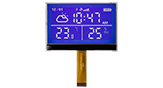
Home Products LCD Display COG LCD Display WO240128A

3.75-inch 240x128 Monochrome Graphic COG LCD Module

Model No. WO240128A

►COG LCD
►Type: Graphic
►Structure: COG
►Size: 3.75"
►Display Format : 240x128 dots
►IC: UC1608
►3V power supply
►1/128 duty cycle
►Interface : 6800/8080/SPI

Description

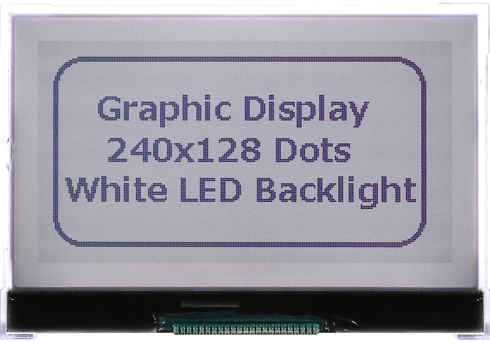
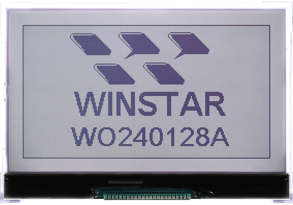
WO240128A is a 3.75-inch 240x128 monochrome graphic COG LCD module featuring the UC1608 controller IC. The display supports 6800, 8080, 3-Line SPI, and 4-Line SPI interfaces with a 3V logic supply.

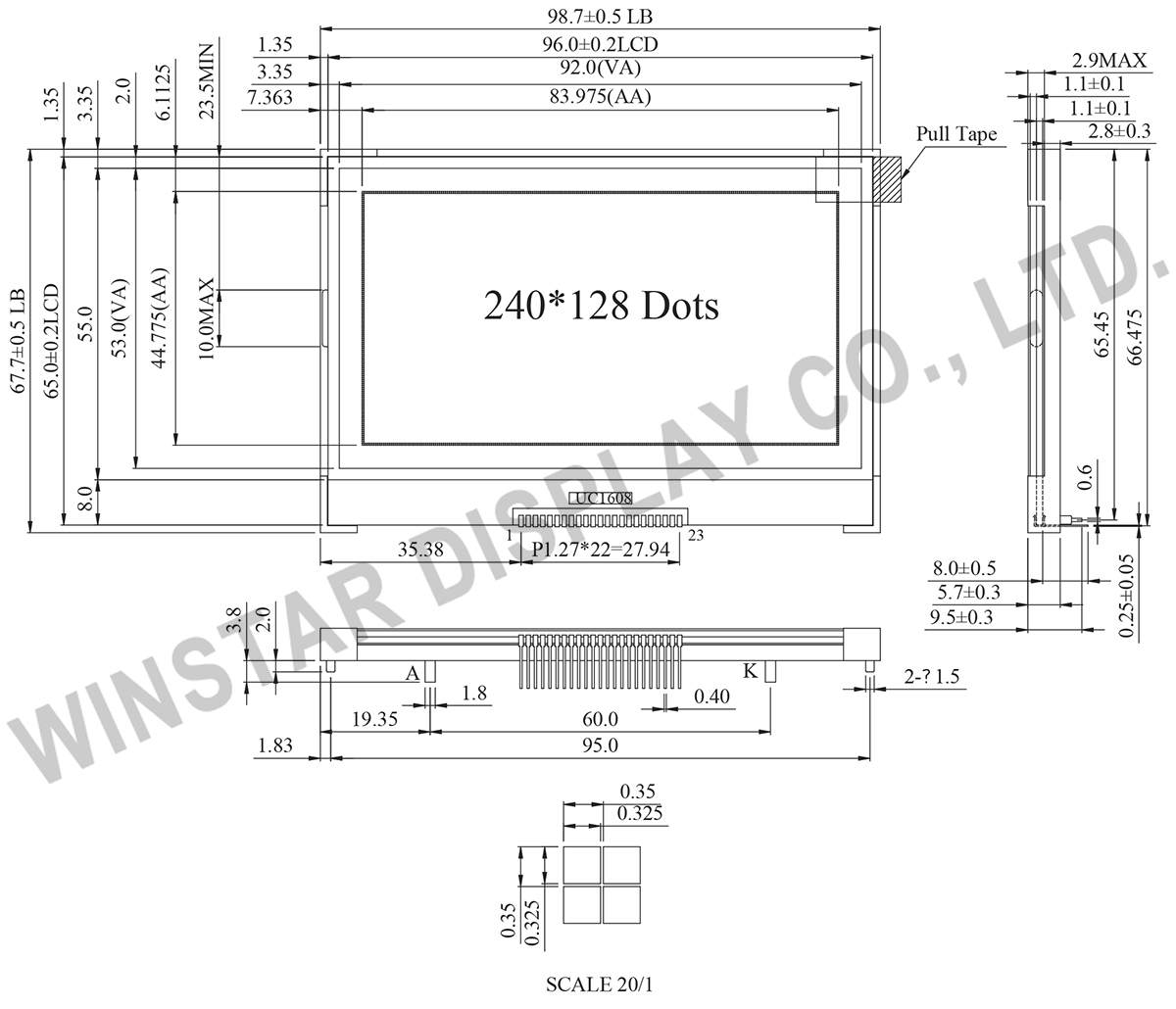
The module measures 98.7 x 67.7 x 9.5 mm, with a 92.0 x 53.0 mm view area and an 83.975 x 44.775 mm active area. It features an LED backlight.

WO240128A combines a 240x128 graphic display with a compact COG design, making it suitable for industrial instruments, medical devices, handheld equipment, and other embedded HMI applications.

Various LCD types and polarizer options are available. Click Add to Inquiry above and specify your requirements in the inquiry message.

DRAWING

WO240128A - Contour Drawing
Data source ref:WO240128A-TFH#

SPECIFICATIONS

Mechanical Data

Item Dimension Unit
Number of Dots 240 x 128 dots
Module dimension 98.7 x 67.7 x 9.5 (Max) mm
View area 92.0 x 53.0 mm
Active area 83.975 x 44.775 mm
Dot size 0.325 x0.325 mm
Dot pitch 0.35 x 0.35 mm
Duty 1/128 , 1/12 Bias
Backlight Type LED
IC UC1608
Interface 6800/8080/3 wire SPI/4 wire SPI

Absolute Maximum Ratings

Item Symbol Min Typ Max Unit
Operating Temperature TOP -20 +70
Storage Temperature TST -30 +80
Supply voltage for Logic VDD -0.3 +4.0 V
LCD Generator supply voltage VDD2 -0.3 +4.0 V
LCD Generated voltage VLCD -0.3 +17.8 V

Electrical Characteristics

Item Symbol Condition Min Typ Max Unit
Supply Voltage For Logic VDD-VSS 2.7 2.8~3.3 3.6 V
Supply Voltage For LCM V0-VSS Ta=-20℃
Ta=25℃
Ta=70℃

15.2

15.5

15.8
V
V
V
Input High Volt. VIH 0.8 VDD V
Input Low Volt. VIL 0.2VDD V
Output High Volt. VOH 0.8VDD V
Output Low Volt. VOL 0.2VDD V
Supply Current(No include LED Backlight) IDD VDD=3.0V 1.1 mA

Interface Pin Function

Pin No. Symbol Type Description
1 VB1- PWR LCD Bias Voltages. These are the voltage source to provide SEG driving currents. These voltages are generated internally. Connect capacitors of CBX between VBX+ and VBX–.
The resistance of these four traces directly affects the SEG driving strength of the resulting LCD module. Minimize the trace resistance is critical in achieving high quality image.
2 VB1+
3 VB0-
4 VB0+
5 VLCD PWR Main LCD Power Supply. Connect these pins together.
6 VBIAS I This is the reference voltage to generate the actual SEG driving voltage. VBIAS can be used to fine tune VLCD by external variable resistors. Internal resistor network has been provided to simplify external trimming circuit.
In COF application, connect a small bypass capacitor between VBIAS and VSS to reduce noise.
7 VSS PWR Ground
8 VDD PWR Supply Voltage for logic
9 D7 I/O Bi-directional bus for both serial and parallel host interfaces.
In serial modes, connect D[0] to SCK, D[3] to SDA,
  BM=1x
(Parallel)
BM=0x
(Parallel)
BM=01
(S9)
BM=00
(S8/S8uc)
D0 D0 D0/D4 SCK SCK
D1 D1 D1/D5 - -
D2 D2 D2/D6 - -
D3 D3 D3/D7 SDA SDA
D4 D4 - - -
D5 D5 - - -
D6 D6 - S9 S8/S8uc
D7 D7 0 1 1
Connect unused pins to VDD or VSS.
10 D6
11 D5
12 D4
13 D3
14 D2
15 D1
16 D0
17 WR1 I WR[1:0] controls the read/write operation of the host interface. See Host Interface section for more detail.
In parallel mode, WR[1:0] meaning depends on whether the interface is in the 6800 mode or the 8080 mode. In serial interface modes, these two pins are not used, connect them to VSS.
18 WR0
19 CD I Select Control data or Display data for read/write operation. In S9 mode, CD pin is not used. Connect CD to VSS when not used. ”L”: Control data ”H”: Display data
20 RST I When RST=”L”, all control registers are re-initialized by their default states.
Since UC1608x has built-in Power-ON-Reset and Software Reset command, RST pin is not required for proper chip operation. When RST is not used, connect the pin to VDD.
21 CS I Chip Select. The chip is selected when CS=”H”. When the chip is not selected, D[7:0] will be high impedance.
22 BM0 I Bus mode: The interface bus mode is determined by BM[1:0] and D[7:6] by the following relationship:
BM[1:0] D[7:6] Mode
11 Data 6800/8-bit
10 Data 8080/8-bit
1 0X 6800/8-bit
0 0X 8080/8-bit
1 10 3-wire SPI w/9-bit token
(S9: conventionl)
0 10 4-wire SPI w/8-bit token
(S8: conventionl)
0 11 3- or 4-wire SPI w/8-bit token
(S8uc: Ultra-Compact)
23 BM1

Search keyword: 240x128 lcd, 240 x 128 lcd, lcd 240x128, lcd 240 x 128

Related Products

go top
close

We value your privacy

By clicking "Allow All Cookies", you agree to the storing of cookies on your device to enhance site navigation, analyse site usage, and assist in our marketing and performance efforts. You can find further information this subject in our policy.

We value your privacy

Winstar and certain third parties use cookies on www.winstar.com.tw. The details regarding the types of
cookies, their purpose and the third parties involved are described below and in our Cookie Policy.
Please click on “Allow All” to consent to our usage of cookies in order to have the best possible
experience on our websites. You can also set your preferences or reject cookies (except for strictly
necessary cookies).

Manage Consent Preferences

Always Active
Essential Cookies

These cookies are essential in order to enable you to move around the website and use its
features, such as setting your privacy preferences, logging in or filling in forms.

Analytics Cookies

Also known as “statistics cookies,” these cookies collect information about how you use a website, like which pages you visited and which links you clicked on. See Detail