
우리는 귀하의 프라이버시를 소중히 여깁니다
"모든 쿠키 허용"을 클릭하면 사이트 탐색을 개선하고, 사이트 사용을 분석하며, 마케팅 및 성능 노력에 도움을 주기 위해 쿠키를 귀하의 장치에 저장하는 데 동의한 것으로 간주됩니다. 이 주제에 대한 추가 정보는 당사의 정책에서 확인할 수 있습니다. 개인정보 보호정책


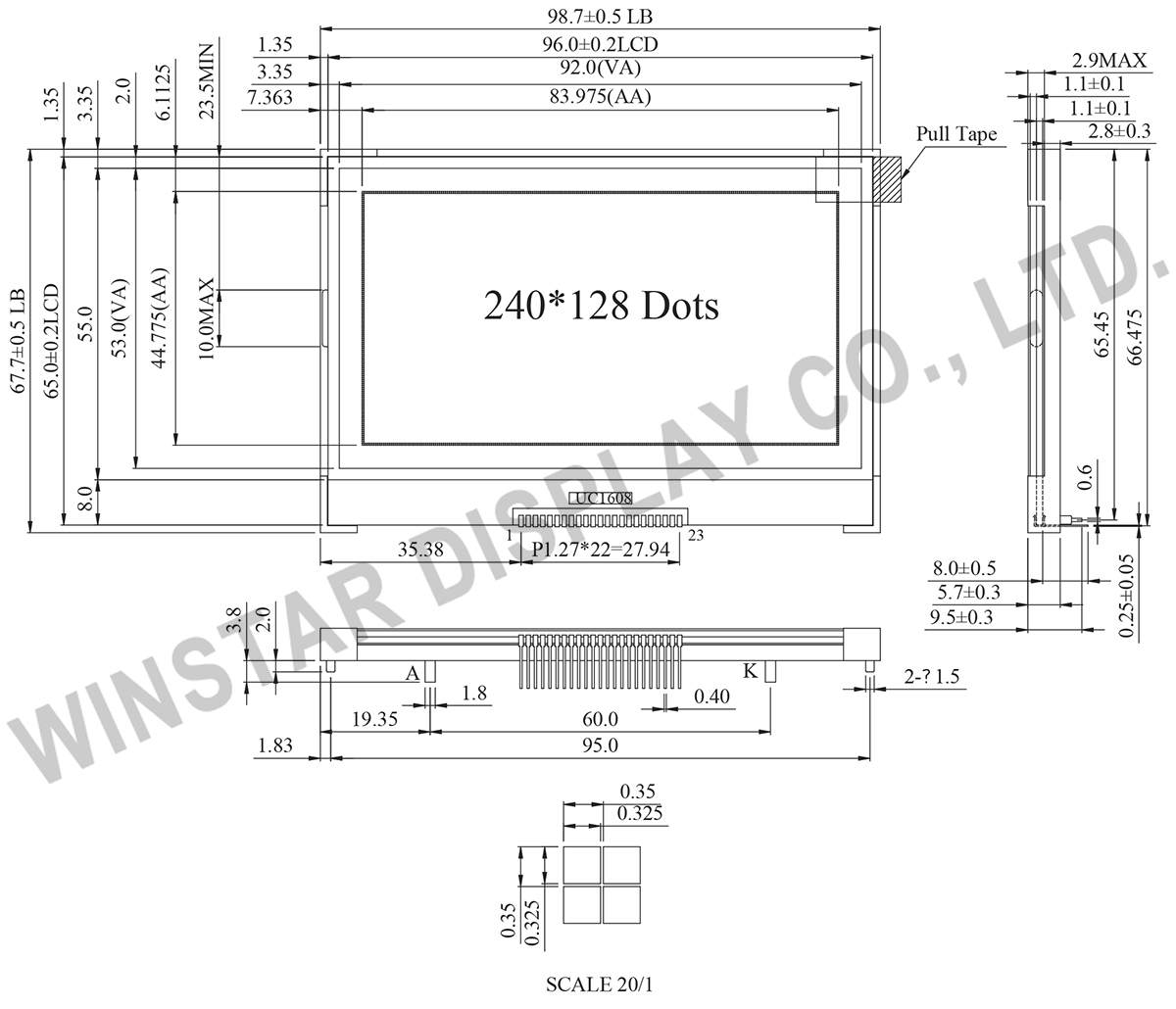
WO240128A는 COG(Chip on Glass) 구조를採用한 3.75인치 모노크롬 그래픽 LCD 모듈로, 240x128 도트의 해상도를 제공합니다. UC1608 컨트롤러 IC가 내장되어 있으며, 6800, 8080, 3선식 SPI, 4선식 SPI 등 다양한 인터페이스를 지원합니다. 이 모듈은 얇고 전력 소모가 적어, 디스플레이 품질과 공간 효율성이 중요한 산업 장비, 의료 기기 및 휴대용 장치 등에 적합합니다. 다양한 LCD 타입과 편광판 옵션이 제공되며, 자세한 사항은 문의해 주세요.
| 항목 | 치수 | 단위 |
|---|---|---|
| 디스플레이 형식 | 240 x 128 점 | - |
| 모듈 치수 | 98.7 x 67.7 x 9.5 (Max) | mm |
| 보기 영역 | 92.0 x 53.0 | mm |
| 활성 영역 | 83.975 x 44.775 | mm |
| 도트 크기 | 0.325 x0.325 | mm |
| 도트 피치 | 0.35 x 0.35 | mm |
| 듀티 | 1/128 , 1/12 Bias | |
| 역광 타입 | LED | |
| IC | UC1608 | |
| 인터페이스 | 6800/8080/3 wire SPI/4 wire SPI | |
| 항목 | 기호 | 최소값 | 대표값 | 최대값 | 단위 |
|---|---|---|---|---|---|
| 작동 온도 | TOP | -20 | - | +70 | ℃ |
| 보관 온도 | TST | -30 | - | +80 | ℃ |
| Supply voltage for Logic | VDD | -0.3 | - | +4.0 | V |
| LCD Generator supply voltage | VDD2 | -0.3 | - | +4.0 | V |
| LCD Generated voltage | VLCD | -0.3 | - | +17.8 | V |
| 항목 | 기호 | 조건 | 최소값 | 대표값 | 최대값 | 단위 |
|---|---|---|---|---|---|---|
| Supply Voltage For Logic | VDD-VSS | - | 2.7 | 2.8~3.3 | 3.6 | V |
| Supply Voltage For LCM | V0-VSS | Ta=-20℃ Ta=25℃ Ta=70℃ |
- 15.2 - |
- 15.5 - |
- 15.8 - |
V V V |
| Input High Volt. | VIH | - | 0.8 VDD | - | - | V |
| Input Low Volt. | VIL | - | - | - | 0.2VDD | V |
| Output High Volt. | VOH | - | 0.8VDD | - | - | V |
| Output Low Volt. | VOL | - | - | - | 0.2VDD | V |
| Supply Current(No include LED Backlight) | IDD | VDD=3.0V | - | 1.1 | - | mA |
| Pin No. | 기호 | Level | 설명 | |||||||||||||||||||||||||||||||||||||||||||||
|---|---|---|---|---|---|---|---|---|---|---|---|---|---|---|---|---|---|---|---|---|---|---|---|---|---|---|---|---|---|---|---|---|---|---|---|---|---|---|---|---|---|---|---|---|---|---|---|---|
| 1 | VB1- | PWR | LCD Bias Voltages. These are the voltage source to provide SEG driving currents. These voltages are generated internally. Connect capacitors of CBX between VBX+ and VBX–. The resistance of these four traces directly affects the SEG driving strength of the resulting LCD module. Minimize the trace resistance is critical in achieving high quality image. |
|||||||||||||||||||||||||||||||||||||||||||||
| 2 | VB1+ | |||||||||||||||||||||||||||||||||||||||||||||||
| 3 | VB0- | |||||||||||||||||||||||||||||||||||||||||||||||
| 4 | VB0+ | |||||||||||||||||||||||||||||||||||||||||||||||
| 5 | VLCD | PWR | Main LCD Power Supply. Connect these pins together. | |||||||||||||||||||||||||||||||||||||||||||||
| 6 | VBIAS | I | This is the reference voltage to generate the actual SEG driving voltage. VBIAS can be used to fine tune VLCD by external variable resistors. Internal resistor network has been provided to simplify external trimming circuit. In COF application, connect a small bypass capacitor between VBIAS and VSS to reduce noise. |
|||||||||||||||||||||||||||||||||||||||||||||
| 7 | VSS | PWR | Ground | |||||||||||||||||||||||||||||||||||||||||||||
| 8 | VDD | PWR | Supply Voltage for logic | |||||||||||||||||||||||||||||||||||||||||||||
| 9 | D7 | I/O | Bi-directional bus for both serial and parallel host interfaces. In serial modes, connect D[0] to SCK, D[3] to SDA,
|
|||||||||||||||||||||||||||||||||||||||||||||
| 10 | D6 | |||||||||||||||||||||||||||||||||||||||||||||||
| 11 | D5 | |||||||||||||||||||||||||||||||||||||||||||||||
| 12 | D4 | |||||||||||||||||||||||||||||||||||||||||||||||
| 13 | D3 | |||||||||||||||||||||||||||||||||||||||||||||||
| 14 | D2 | |||||||||||||||||||||||||||||||||||||||||||||||
| 15 | D1 | |||||||||||||||||||||||||||||||||||||||||||||||
| 16 | D0 | |||||||||||||||||||||||||||||||||||||||||||||||
| 17 | WR1 | I | WR[1:0] controls the read/write operation of the host interface. See Host Interface section for more detail. In parallel mode, WR[1:0] meaning depends on whether the interface is in the 6800 mode or the 8080 mode. In serial interface modes, these two pins are not used, connect them to VSS. |
|||||||||||||||||||||||||||||||||||||||||||||
| 18 | WR0 | |||||||||||||||||||||||||||||||||||||||||||||||
| 19 | CD | I | Select Control data or Display data for read/write operation. In S9 mode, CD pin is not used. Connect CD to VSS when not used. ”L”: Control data ”H”: Display data | |||||||||||||||||||||||||||||||||||||||||||||
| 20 | RST | I | When RST=”L”, all control registers are re-initialized by their default states. Since UC1608x has built-in Power-ON-Reset and Software Reset command, RST pin is not required for proper chip operation. When RST is not used, connect the pin to VDD. |
|||||||||||||||||||||||||||||||||||||||||||||
| 21 | CS | I | Chip Select. The chip is selected when CS=”H”. When the chip is not selected, D[7:0] will be high impedance. | |||||||||||||||||||||||||||||||||||||||||||||
| 22 | BM0 | I | Bus mode: The interface bus mode is determined by BM[1:0] and D[7:6] by the following relationship:
|
|||||||||||||||||||||||||||||||||||||||||||||
| 23 | BM1 |

"모든 쿠키 허용"을 클릭하면 사이트 탐색을 개선하고, 사이트 사용을 분석하며, 마케팅 및 성능 노력에 도움을 주기 위해 쿠키를 귀하의 장치에 저장하는 데 동의한 것으로 간주됩니다. 이 주제에 대한 추가 정보는 당사의 정책에서 확인할 수 있습니다. 개인정보 보호정책