Home Products TFT Display Standard TFT Color Display WF28KTZAJDNG0

2.8-inch TFT LCD with PCAP Touch Panel & O-Film

Model No. WF28KTZAJDNG0

►Size: 2.8"
►Resolution: 240 x 320 dots
►View Direction: O-TFT (75/75/75/75)
►Interface: SPI
►Driver IC:ST7789V
►Control-Board: No
►Brightness(cd/m²): 350
►Frame Through Hole: No
►Touch Panel: Projected Capacitive Touch Panel (PCAP)
►Detect Point : 1 Finger

Description

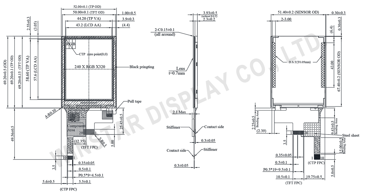
The WF28KTZAJDNG0 is a 2.8-inch TFT LCD display module with a projected capacitive (PCAP) touch panel, specifically designed for industrial applications. It features a resolution of 240 x 320 pixels in portrait orientation, making it ideal for compact, space-constrained devices. The module is equipped with the ST7789V driver IC for the TFT display, which supports an SPI interface, ensuring fast and reliable data communication.

The PCAP touch panel uses the CF1124 driver IC and supports an I2C interface. It offers 1-point touch detection, making it suitable for user interfaces that require simple and responsive touch interaction.

This display incorporates O-Film, which enhances its viewing angles to 75° in all directions (left, right, up, down), ensuring clear visibility from multiple perspectives. This makes it an excellent choice for applications where viewing from various angles is important.

This module is especially suitable for industrial applications such as portable medical monitors, where durability and long operational lifetimes are essential. With its robust design, the WF28KTZAJDNG0 is engineered to provide reliable performance for 5 to 6 years of continuous use.

DRAWING

2.8-inch TFT LCD with PCAP Touch Panel & O-Film - WF28KTZAJDNG0

SPECIFICATIONS

General Specifications

Item Dimension Unit
Size 2.8 inch
Dot Matrix 240 × RGB × 320(TFT) dots
Module dimension 50.0(W) × 69.2(H) × 3.93(D) mm
Active area 43.2 × 57.6 mm
Dot pitch 0.18 × 0.18 mm
LCD type TFT, Normally White, Transmissive
TFT Interface SPI
Driver IC ST7789V or Equivalent
View Angle 75/75/75/75
Aspect Ratio Portrait
Backlight Type LED, Normally White
PCAP Driver IC CF1124 or Equivalent
PCAP Interface I2C
PCAP FW Version 01
PCAP Resolution 240*320
Touch Panel Projected Capacitive Touch Panel (PCAP)
Surface Glare

Absolute Maximum Ratings

Item Symbol Min Typ Max Unit
Operating Temperature TOP -20 +70
Storage Temperature TST -30 +80

Electrical Characteristics

Operating conditions

Item Symbol Min Typ Max Unit
Supply Voltage For Analog VCC 2.4 3.3 3.6 V
Supply Current For LCM ICC 6.7 10.0 mA
Supply Voltage For Touch Logic VDDT 3.0 3.3 3.6 V
IDDT 15 25 V
 

LED driving conditions

Parameter Symbol Min Typ Max Unit
LED current   - 80 - mA
Power Consumption   232 256 272 mW
LED voltage VBL+ 2.9 3.2 3.4 V
LED Life Time   50,000 - - Hr

Interface

LCM PIN Definition

NO Symbol Function
1 GND Ground
2 VLED+ Anode of LED backlight.
3 VLED- Cathode of LED backlight.
4 GND Ground
5 VCC Power supply
6 RESET System reset pin. (RESX)
signal is active low
7 SDA When IM3: Low, SPI interface input/output pin.
When IM3: High, SPI interface input pin.
The data is latched on the rising edge of the SCL signal.
If not used, please fix this pin at VDDI or DGND level.
8 DCX(SCL) This pin is used to be serial interface clock.
DCX=’1’: display data or parameter.
DCX=’0’: command data.
If not used, please fix this pin at VDDI or DGND.
9 CSX Chip selection pin
Low enable.
High disable.
10 WRX(D/CX) Display data/command selection pin in 4-line serial interface.
Second Data lane in 2 data lane serial interface.
If not used, please fix this pin at VDDI or DGND.
11 GND Ground
12 SDO(DOUT) SPI interface output pin.
The data is output on the falling edge of the SCL signal.
If not used, let this pin open.
13 TE Tearing effect signal is used to synchronize MCU to frame memory
writing.
If not used, please let this pin open
14 IM3 The MCU interface mode select.
IM3 IM2 IM1 IM0 MPU Interface Mode Data pin
0 1 1 0 4-lin 8bit serial I/F SDA: in/out
1 1 1 0 4-lin 8bit serial I/F Ⅱ SDA: in/
SDO:out
15 GND Ground
16-19 NC No connect
20 GND Ground
 

PCAP PIN Definition

Pin Symbol Function
1 VSS Ground for analog circuit
2 VDDT Power Supply : +3.3V
3 SCL I2C clock input
4 NC No connect
5 SDA I2C data input and output
6 NC No connect
7 /RST External Reset, Low is active
8 NC No connect
9 /INT External interrupt to the host
10 VSS Ground for analog circuit
go top
close

We value your privacy

By clicking "Allow All Cookies", you agree to the storing of cookies on your device to enhance site navigation, analyse site usage, and assist in our marketing and performance efforts. You can find further information this subject in our policy.

We value your privacy

Winstar and certain third parties use cookies on www.winstar.com.tw. The details regarding the types of
cookies, their purpose and the third parties involved are described below and in our Cookie Policy.
Please click on “Allow All” to consent to our usage of cookies in order to have the best possible
experience on our websites. You can also set your preferences or reject cookies (except for strictly
necessary cookies).

Manage Consent Preferences

Always Active
Essential Cookies

These cookies are essential in order to enable you to move around the website and use its
features, such as setting your privacy preferences, logging in or filling in forms.

Analytics Cookies

Also known as “statistics cookies,” these cookies collect information about how you use a website, like which pages you visited and which links you clicked on. See Detail