Home Products TFT Display IPS TFT LCD WF70A8TYAHMNN0

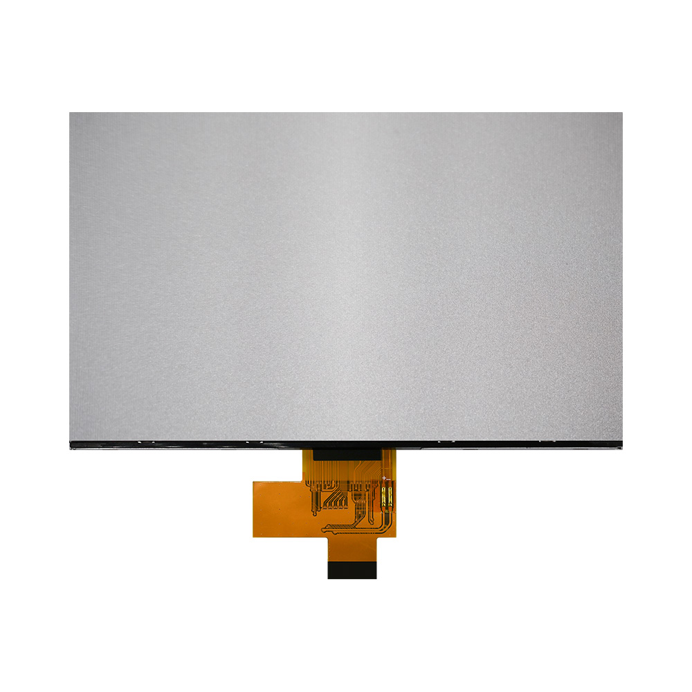
7 inch 1024x600 MIPI IPS TFT Display

Model No. WF70A8TYAHMNN0

►Size : 7 inch
►Resolution : 1024 x 600 dots
►View Direction : IPS
►Interface : 4-Lanes MIPI
►Driver IC : EK79007AD3 + EK73217BCGA
►Control-Board : No
►Brightness(cd/m2): 600
►Frame Through Hole : No
►Touch Screen : No

Description

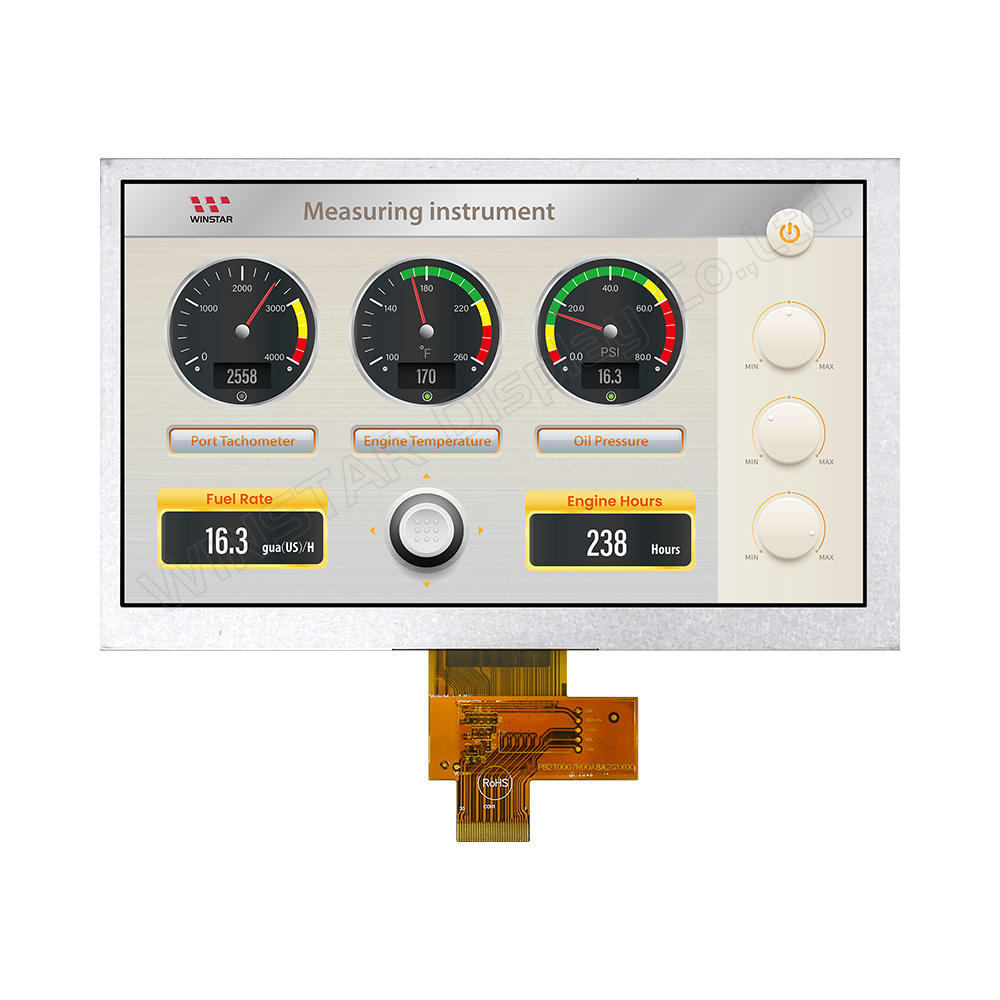
The WF70A8TYAHMNN0 is a 7-inch MIPI DSI interface 1024x600 IPS TFT-LCD module. Featuring IPS technology, this module delivers superior image quality with wide viewing angles of 85° left, 85° right, 85° up, and 85° down, ensuring that the display remains clear and vivid from virtually any perspective. The contrast ratio is 800:1 (typical value), and the brightness is 600 cd/m² (typical value). The anti-glare surface panel minimizes reflections, enhancing visibility in bright environments. With a 16:9 aspect ratio, this module is ideal for applications that require sharp, clear images.

For customers who need even higher brightness, the WF70A8SYAHMNN0 model, offering 1100 cd/m², is also available.

The WF70A8 series comes in both projected capacitive touch panel (PCAP) and resistive touch panel (RTP) options, and is also available with an LVDS interface, providing flexibility for different system integration needs. For more information on specific models, please feel free to contact us through our website.

The WF70A8TYAHMNN0 module is powered by EK7900AD3 and EK73217BCGA driver ICs, supporting a 4-lane MIPI DSI (Mobile Industry Processor Interface) for high-speed data and clock transmission, ensuring faster, more reliable performance.

This module operates within a temperature range of -20°C to +70°C, with storage temperatures ranging from -30°C to +80°C, making it suitable for a wide range of industrial and outdoor applications.

 

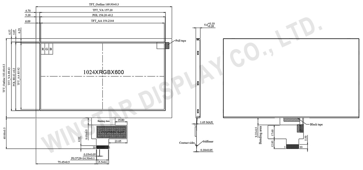
DRAWING

7 inch 1024x600 MIPI IPS TFT Display - WF70A8TYAHMNN0

SPECIFICATIONS

General Specifications

Item Dimension Unit
Size 7.0 inch
Dot Matrix 1024 × RGB × 600(TFT) dots
Module dimension 169.9(W) × 103.4(H) × 5.6(D) mm
Active area 154.2114 × 85.92 mm
Dot pitch 0.1506 × 0.1432 mm
LCD type TFT, Normally White, Transmissive
View Direction 85/85/85/85
Aspect Ratio 16:9
Driver IC EK79007AD3 + EK73217BCGA or equivalent
Interface 4-Lanes MIPI
Backlight Type LED, Normally White
Touch Screen Without touch screen
Surface Anti-Glare

Absolute Maximum Ratings

Item Symbol Min Typ Max Unit
Operating Temperature TOP -20 +70
Storage Temperature TST -30 +80

Electrical Characteristics

Typical Operation Conditions

Item Symbol Values Unit
Min. Typ. Max.
Power voltage VDD 1.71 1.8 1.89 V
Analog Power AVDD 8.9 9.0 9.1 V
TFT Gate ON Voltage VGH 17 18 19 V
TFT Gate OFF Voltage VGL -6.5 -6.0 -5.5 V
TFT Common Voltage VCOMIN 3.0 3.15 3.3 V
Current for Driver IDD -- 16 24 mA
Power Current IAVDD -- 19 28.5 mA
TFT Gate ON Current IVGH -- 1.6 2.4 mA
TFT Gate OFF Current IVGL -- 0.6 0.9 mA
TFT Common Current IVCOMIN -- 0 -- mA
 

Backlight Driving Conditions

Item Symbol Values Unit
Min. Typ. Max.
Voltage for LED backlight VL 16.8 19.2 21.0 V
Current for LED backlight IL -- 240 -- mA
LED life time - - 50,000 - Hr

Interface

LCM PIN Definition

Pin No. Symbol Function
1 VLED+ LED Anode
2 VLED+ LED Anode
3 VGH Positive power for TFT
4 VGL Negative power for TFT
5 UPDN Gate up or down scan control.
UPDN = ”L”, STV2 output vertical start pulse and UD pin output logical “L” to Gate driver. (default)
UPDN = ”H”, STV1 output vertical start pulse and UD pin output logical “H” to Gate driver
6 SHLR Source right or left sequence control.
SHLR = ”L“, shift left: last data = S1←S2←S3….......←S1536 = first data.
SHLR = ”H“, shift right: first data = S1→S2→S3….....→S1536 = last data.(default)
7 VLED- LED Cathode
8 VLED- LED Cathode
9 AVDD Power for Analog Circuit
10 GND Ground
11 D3P MIPI data input.
12 D3N MIPI data input.
13 GND Ground
14 D2P MIPI data input.
15 D2N MIPI data input.
16 GND Ground
17 CLKP MIPI clock input
18 CLKN MIPI clock input
19 GND Ground
20 D1P MIPI data input.
21 D1N MIPI data input.
22 GND Ground
23 D0P MIPI data input.
24 D0N MIPI data input.
25 GND Ground
26 STBYB Standby mode.
STBYB = ”H“,normal operation(default)
STBYB = ”L”, timing controller, source driver will turn off, all output are GND.
27 RESET Global reset pin. Active Low to enter Reset State. Normally pull high. Connecting with an RC reset circuit for stability.
28 VDD(1.8V) Digital circuit
29 VDD(1.8V) Digital circuit
30 VCOMIN Common voltage

Related Products

go top
close

We value your privacy

By clicking "Allow All Cookies", you agree to the storing of cookies on your device to enhance site navigation, analyse site usage, and assist in our marketing and performance efforts. You can find further information this subject in our policy.

We value your privacy

Winstar and certain third parties use cookies on www.winstar.com.tw. The details regarding the types of
cookies, their purpose and the third parties involved are described below and in our Cookie Policy.
Please click on “Allow All” to consent to our usage of cookies in order to have the best possible
experience on our websites. You can also set your preferences or reject cookies (except for strictly
necessary cookies).

Manage Consent Preferences

Always Active
Essential Cookies

These cookies are essential in order to enable you to move around the website and use its
features, such as setting your privacy preferences, logging in or filling in forms.

Analytics Cookies

Also known as “statistics cookies,” these cookies collect information about how you use a website, like which pages you visited and which links you clicked on. See Detail