5.7" Resistive Touch TFT-LCD
Model No. WF57XTIACDNT0
►Size : 5.7 inch
►Resolution : 320 x 240 dots
►View Direction : 12H
►Interface : RGB
►Driver IC:HX8218+HX8615
►Control-Board : Option
►Brightness(cd/m²): 600
►Frame Through Hole : No
►Touch Screen : Resistive Touch Panel
►O-Film : Option
Description
The WF57XTIACDNT0 is a 5.7-inch TFT LCD module equipped with a Resistive Touch Panel, featuring a resolution of 320 x 240 dots. Its brightness has been optimized to 600 cd/m², while adopting an Anti-Glare surface for enhanced readability in various lighting conditions.
Driven by the HX8218+HX8615 driver IC, this module supports 24-bit RGB interfaces, ensuring vibrant and accurate color representation. With a voltage power supply ranging from 3.2V to 3.4V (typical value: 3.3V), it maintains efficient operation.
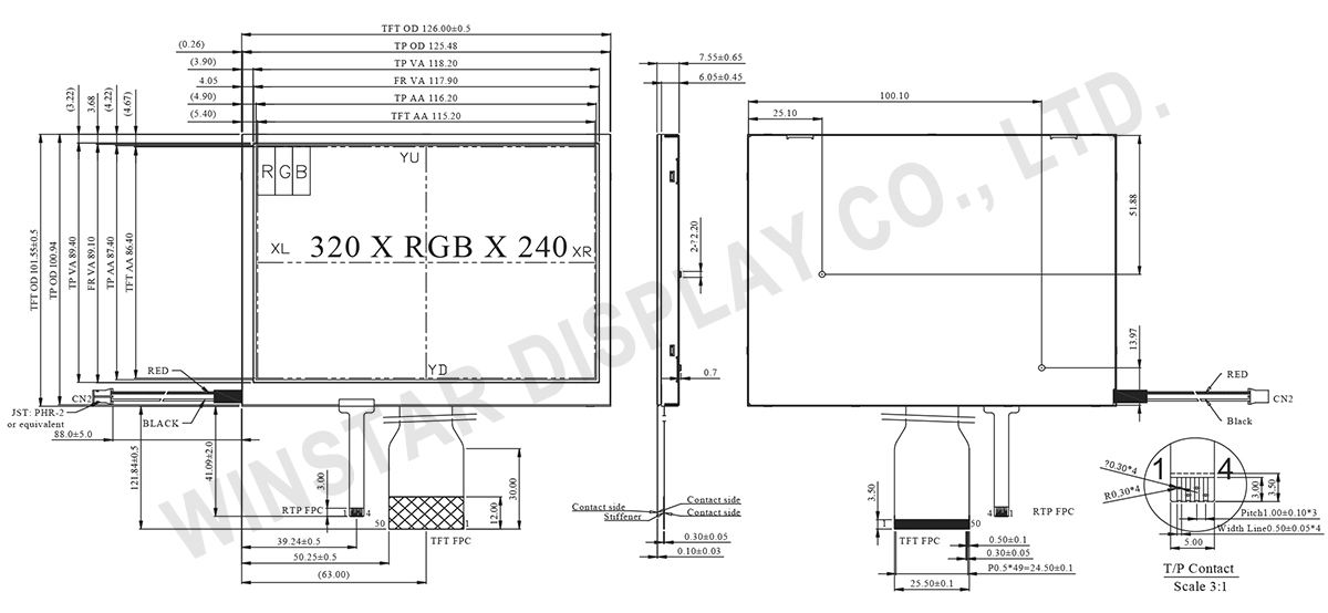
The module's dimensions measure 126.00(W) × 101.55(H) mm, with an active area of 115.2 × 86.40 mm, making it suitable for compact applications. It maintains a 4:3 aspect ratio, ideal for a wide range of display needs.
Featuring a 12 o'clock viewing direction and a 6 o'clock gray scale inversion direction, this TFT display offers versatile usability. It operates reliably within a temperature range of -20℃ to +70℃, with a storage temperature ranging from -30℃ to +80℃, ensuring durability in various environments.
The WF57XTIACDNT0 is well-suited for applications requiring clear and responsive displays, such as Industrial Control and Monitoring systems. The Resistive Touch Panel adds interactivity, enhancing user experience and functionality. Its Anti-Glare surface minimizes reflections, ensuring optimal visibility even in bright light conditions.
DRAWING
SPECIFICATIONS
Interface
LCM PIN Definition
Pin No. | Symbol | I/O | Description |
---|---|---|---|
1 | IF1 | I | Input data format control (Note1) |
2 | IF2 | I | Input data format control (Note1) |
3 | POL | O | Polarity Signal connect to VCOM driving circuit. |
4 | RESET | I | Hardware reset. |
5 | SPENA | I | Chip select |
6 | SPCL | I | Serial Clock |
7 | SPDA | I/O | Serial Data |
8 | B0 | I | Blue Data bit (LSB) |
9 | B1 | I | Blue Data bit |
10 | B2 | I | Blue Data bit |
11 | B3 | I | Blue Data bit |
12 | B4 | I | Blue Data bit |
13 | B5 | I | Blue Data bit |
14 | B6 | I | Blue Data bit |
15 | B7 | I | Blue Data bit(MSB) |
16 | G0 | I | Green Data bit(LSB) |
17 | G1 | I | Green Data bit |
18 | G2 | I | Green Data bit |
19 | G3 | I | Green Data bit |
20 | G4 | I | Green Data bit |
21 | G5 | I | Green Data bit |
22 | G6 | I | Green Data bit |
23 | G7 | I | Green Data bit(MSB) |
24 | R0 | I | Red Data bit(LSB) |
25 | R1 | I | Red Data bit |
26 | R2 | I | Red Data bit |
27 | R3 | I | Red Data bit |
28 | R4 | I | Red Data bit |
29 | R5 | I | Red Data bit |
30 | R6 | I | Red Data bit |
31 | R7 | I | Red Data bit(MSB) |
32 | Hsync | I | Horizontal synchronous signal |
33 | Vsync | I | Vertical synchronous signal |
34 | Data CLK | I | Dot data clock |
35 | AVDD | I | 4.5V~5.5V |
36 | AVDD | I | 4.5V~5.5V |
37 | Vcc | I | 3V~3.6V |
38 | Vcc | I | 3V~3.6V |
39 | NPC | O | NTSC/PAL mode Auto detection result H:NTSC/L:PAL |
40 | VGL | I | Gate off power |
41 | VGL | I | Gate off power |
42 | UD | I | Up/Down scan setting. H: Reverse scan / L: Normal scan |
43 | VGH | I | Gate on power |
44 | LRC | I | Shift direction of device internal shift register control. |
45 | GND | I | GROUND |
46 | VCOM | I | VCOM driving input |
47 | VCOM | I | VCOM driving input |
48 | ENB | I | Data enable input. Normally pull low. |
49 | GND | I | GROUND |
50 | GND | I | GROUND |
General Specifications
Item | Dimension | Unit |
---|---|---|
Size | 5.7 | inch |
Dot Matrix | 320 × RGB × 240 (TFT) | dots |
Module dimension | 126.00(W) × 101.55(H) × 8.15(D)(MAX) | mm |
Active area | 115.2 × 86.40 | mm |
Dot pitch | 0.12 × 0.36 | mm |
LCD type | TFT, Normally White, Transmissive | |
View Direction | 12 o'clock | |
Gray Scale Inversion Direction | 6 o'clock | |
Aspect Ratio | 4:3 | |
TFT Drive IC | HX8218+HX8615 or Equivalent | |
Interface | 24-bit RGB | |
Backlight Type | LED, Normally White | |
Touch Panel | Resistive Touch Panel | |
Surface | Anti-Glare |
Absolute Maximum Ratings
Item | Symbol | Min | Typ | Max | Unit |
---|---|---|---|---|---|
Operating Temperature | TOP | -20 | - | +70 | ℃ |
Storage Temperature | TST | -30 | - | +80 | ℃ |
Electrical Characteristics
1. Operating conditions:Item | Symbol | Condition | Min | Typ | Max | Unit |
---|---|---|---|---|---|---|
Supply Voltage For LCM | VCC | - | 3.2 | 3.3 | 3.4 | V |
AVDD | 4.5 | 5.0 | 5.5 | |||
Input High Volt. | VIH | - | 0.7 VCC | - | VCC | V |
Input Low Volt. | VIL | - | 0 | - | 0.3 VCC | V |
LCD Driving Supply Voltage | VGH | Ta=25℃ | 15 | 16 | 17 | V |
VGL | -6 | -5 | -4 | |||
VcomH | - | 4.5 | - | |||
VcomL | - | -0.5 | - | |||
Supply Current For LCM | IVCC | VCC=3.3V | - | 30 | 45 | mA |
2. LED driving conditions
Parameter | Symbol | Min | Typ | Max | Unit |
---|---|---|---|---|---|
LED current | - | - | 140 | - | mA |
Power Consumption | - | 1204 | - | 1470 | mW |
LED voltage | VBL+ | 8.6 | 9.5 | 10.5 | V |
LED Life Time | - | - | 50,000 | - | Hr |