Modern embedded and industrial electronic systems often operate from multiple power sources within increasingly complex power distribution architectures. As system complexity grows, protecting the power input becomes essential to maintaining reliable operation during abnormal conditions such as reverse polarity, hot-plug events, short circuits, overloads, and supply interruptions.
For example, when a storage device is hot-swapped, the resulting inrush current can cause a temporary voltage drop on the shared power rail, potentially affecting other loads connected to the same supply. Proper input power protection helps isolate these disturbances, improving overall system reliability and preventing unexpected shutdowns.
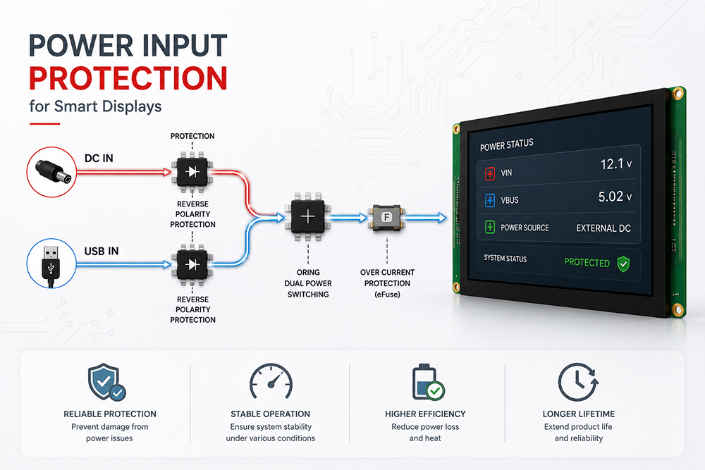
A typical front-end power protection design incorporates three fundamental functions: reverse polarity protection, reverse current blocking (ORing), and overcurrent protection.
The protection techniques described in this article reflect widely adopted power design practices for electronic systems. Depending on system architecture and application requirements, selected WINSTAR Smart Display models incorporate these techniques to improve power integrity and overall system reliability.
1. Reverse Polarity Protection Using a Schottky Diode
Schottky diodes provide one of the simplest and most widely used methods of reverse polarity protection. When the input supply is connected with the correct polarity, the diode conducts normally. If the supply polarity is reversed, the diode becomes reverse-biased and blocks current from reaching the downstream circuitry, preventing damage caused by incorrect power connections.
Because of their simple implementation and low component cost, Schottky diodes are commonly used in low-current applications where efficiency is not the primary design objective. However, the forward voltage drop inherent to the diode introduces conduction loss, reducing overall power efficiency. This becomes increasingly significant as load current increases.
For example, an SM5819 Schottky diode typically exhibits a forward voltage drop of approximately 0.6 V. In a system drawing 3 A, the resulting power dissipation is approximately 1.8 W (0.6 V × 3 A). Selecting a diode with a lower forward voltage can reduce power loss, although this is often accompanied by higher device cost and increased reverse leakage current.
Schottky diode protection is therefore well suited to applications requiring a simple, low-cost input protection solution.
Advantages: Simple circuit implementation and low component cost.
Limitations: Forward voltage drop results in power loss and heat generation, while reverse leakage current increases at elevated temperatures. As load current increases, conduction loss becomes more significant, reducing overall system efficiency and potentially affecting long-term reliability.
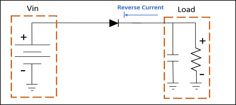
Figure 1. Reverse Polarity Protection Circuit Using a Schottky Diode
2. Reverse Polarity Protection Using a PMOS Ideal Diode
A PMOS transistor is commonly used to implement an ideal diode for reverse polarity protection while significantly reducing conduction loss compared with a Schottky diode. During normal operation, the PMOS body diode initially conducts until the gate-to-source voltage (VGS) becomes sufficiently negative to fully enhance the MOSFET. Once fully turned on, current flows through the low-resistance channel rather than the body diode, minimizing forward voltage drop and improving overall power efficiency. If the input polarity is reversed, the PMOS remains off, preventing reverse current from reaching the downstream circuitry.
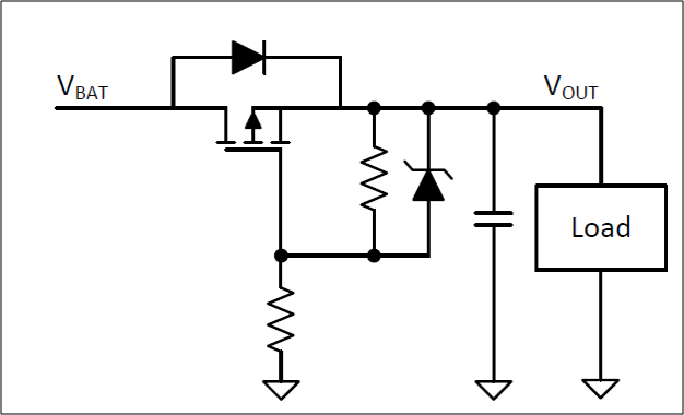
Figure 2. Reverse Polarity Protection Using a PMOS Ideal Diode
Standby Power Considerations
Conventional PMOS reverse polarity protection circuits typically use a resistor to pull the gate toward ground. A Zener diode is often added between the gate and source to limit the gate-to-source voltage (VGS) and protect the MOSFET during input voltage transients. Although this approach is widely used, both the Zener diode and the associated resistor introduce leakage current, increasing standby power consumption.
Selecting an excessively large gate resistor further reduces gate drive current, slowing the PMOS turn-on process. As a result, the MOSFET may remain in its linear operating region longer than intended, increasing switching loss and thermal stress.
Reverse Current During Supply Interruption
Under ISO 16750-2 input voltage interruption conditions, systems with large output capacitors may experience reverse current when the input supply collapses. The energy stored in the output capacitor can temporarily drive current back toward the input through the PMOS body diode before the device completely blocks conduction. Repeated charge and discharge cycles may increase thermal stress, particularly when large electrolytic capacitors are used.
Design Considerations
- Leakage current in the gate protection network increases standby power consumption.
- Insufficient Zener clamping may expose the MOSFET to excessive gate-to-source voltage (VGS).
- Insufficient gate drive current can increase switching time and device heating.
PMOS ideal diode circuits are widely used for input power protection in applications where higher efficiency is required.
Advantages: Lower conduction loss than Schottky diode solutions while maintaining a simpler implementation than eFuse-based protection.
Limitations: Higher component cost than Schottky diode solutions and additional gate-drive design considerations.
Applications requiring automatic source selection or redundant power inputs often adopt an ORing architecture to further improve system reliability.
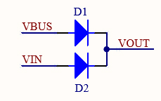
Figure 3. ORing Dual Power Switching Circuit Using Schottky Diodes
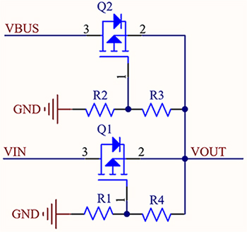
Figure 4. ORing Dual Power Switching Circuit Using PMOS
ORing Power Architecture for Automatic Power Source Selection
ORing power architectures are widely used in systems with multiple power sources, such as an external power supply and a USB input or a backup battery. Instead of relying on a single protection device, the ORing configuration automatically selects the power source with the higher voltage while preventing reverse current between supplies.
Each power path behaves as an ideal diode, allowing current to flow only toward the load. This prevents cross-conduction between supplies and enables seamless source transitions without generating circulating current.
In the example shown above, power switching operates as follows:
- When both VIN and VBUS are available, VIN has priority and supplies power to VOUT, while the VBUS path remains blocked.
- If VIN is removed, the circuit automatically transfers the load to VBUS without interrupting system operation.
- When VIN is restored, the circuit automatically switches the load back to VIN. In the Schottky diode implementation, current flows through D2 when VIN exceeds VBUS and through D1 when VIN is unavailable. In the PMOS implementation, Q1 conducts when VIN is active, while Q2 supplies the load whenever VIN is absent.
The ORing dual-power switching circuit described in this article is covered by a utility model patent. The ORing architecture itself, however, is a well-established power management technique widely adopted in electronic systems.
3. Overcurrent Protection Using an eFuse
For applications requiring a higher level of protection, an electronic fuse (eFuse) provides a more comprehensive solution than discrete protection circuits. In addition to overcurrent protection, modern eFuse devices integrate reverse polarity protection, reverse current blocking, and multiple programmable protection features within a single IC.
Most industrial eFuse devices incorporate back-to-back MOSFETs to prevent reverse current during input power interruptions or voltage brownout conditions. This architecture allows the output voltage to remain isolated from the input supply, helping protect both the power source and downstream circuitry.
In addition to current limiting, eFuse devices typically provide programmable output slew-rate control, adjustable overvoltage (OVP) and undervoltage (UVLO) thresholds, and fault reporting functions. Dedicated enable pins allow the internal MOSFETs to be turned on or off externally while supporting an ultra-low standby current shutdown mode. Status outputs and current-monitoring functions also simplify system diagnostics and power management.
Many industrial eFuse ICs further provide multiple fault-response modes, such as circuit breaker, latch-off, or automatic retry, allowing designers to optimize system behavior for different applications. Their wide input voltage range also simplifies surge protection design in demanding industrial environments.
Advantages: Integrates overvoltage (OVP), overcurrent (OCP), overtemperature (OTP), reverse current blocking, and fast fault protection in a single device. The low on-resistance of the integrated MOSFETs minimizes power dissipation while improving overall system efficiency.
Limitations: Higher component cost compared with discrete protection solutions.
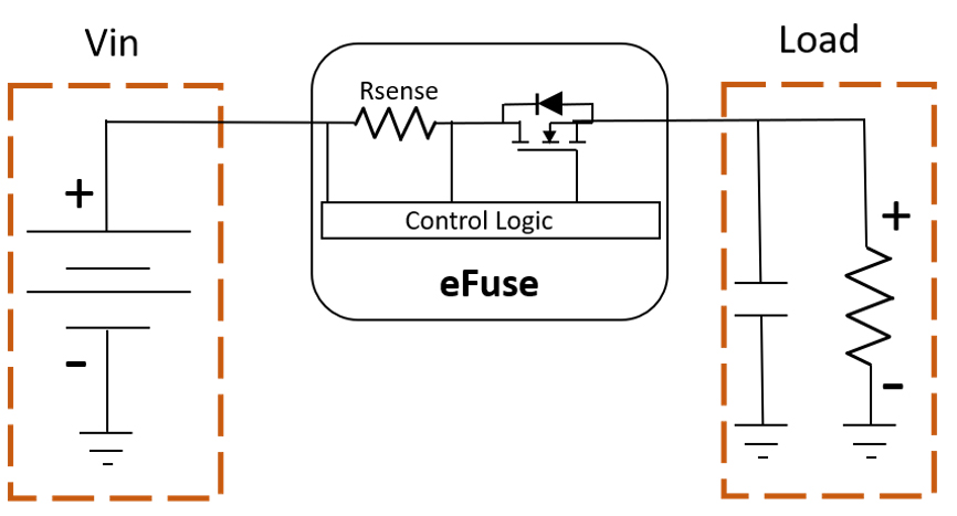
Figure 5. Input Power Protection Architecture Using an eFuse
No single protection method is suitable for every application. Depending on system requirements, designers may choose Schottky diodes, PMOS ideal diodes, ORing architectures, or eFuse devices to achieve the desired balance between efficiency, protection capability, cost, and system reliability. Selecting the appropriate input power protection strategy is an important step toward building robust industrial and embedded systems.
Frequently Asked Questions (FAQ)
1. Why is input power protection important for smart displays?
Smart displays are commonly deployed in industrial automation, medical equipment, transportation systems, and embedded devices where power abnormalities such as reverse polarity, overcurrent, hot-plug events, and voltage transients may occur. A properly designed input power protection circuit helps prevent system failures, improves power stability, and enhances overall product reliability and service life.
2. What is the difference between a Schottky diode and a PMOS ideal diode?
Schottky diodes offer a simple and cost-effective solution for reverse polarity protection but introduce forward voltage drop and power loss. PMOS ideal diode circuits significantly reduce conduction loss and improve power efficiency, making them suitable for applications where energy efficiency is more critical. The trade-off is increased circuit complexity and higher component cost.
3. When should an ORing power architecture be used?
ORing power architectures are commonly used in systems with multiple power sources, such as an external DC supply and USB power, or a primary supply with a backup battery. They automatically select the available power source while preventing reverse current and cross-conduction between supplies, ensuring uninterrupted system operation.
4. How does an eFuse differ from a conventional fuse?
Unlike conventional fuses, eFuse devices integrate multiple protection functions into a single IC. In addition to overcurrent protection, they typically provide overvoltage (OVP), undervoltage (UVLO), overtemperature (OTP), reverse current blocking, programmable current limiting, and configurable fault response, making them well suited for industrial and embedded power management applications.
5. How can reverse current be prevented when USB and an external power supply are connected simultaneously?
Reverse current can be effectively prevented by using an ORing architecture, a PMOS ideal diode circuit, or an eFuse with reverse current blocking. These solutions automatically manage power source selection while preventing current from flowing between different power inputs.
6. How can the reliability of a smart display power system be improved?
A robust input power protection design typically combines reverse polarity protection, reverse current blocking, and overcurrent protection. Selecting the appropriate combination of Schottky diodes, PMOS ideal diodes, ORing architectures, or eFuse devices according to system requirements helps improve power integrity, increase system reliability, and extend product lifetime.
References
The information presented in this article is based on publicly available technical documentation and reference materials, including the following sources.
Semiconductor Manufacturer Technical Documentation
- Texas Instruments — Basics of Ideal Diodes (Rev. B)
- Texas Instruments — Reverse Battery Protection for High Side Switches
- Texas Instruments — Basics of eFuses (Rev. A)
- Nexperia — IAN50001: Automotive Reverse Battery Protection
- Monolithic Power Systems (MPS) — Designing a Reverse Polarity Protection Circuit (Part 1)
- Coil Technology Corporation — Reverse Current Protection
Additional Technical References
- Dianlua — MOSFET Reverse Polarity Protection Circuit
- Dianlua — Automatic Power Switching Between USB and Rechargeable Battery Supplies
- Well Tsai — Reverse Voltage Protection: Comparing Diode and P-MOSFET Solutions
- Alibaba Cloud Developer Community — Automatic Power Switching Circuit Overview