

我們重視您的隱私
通過點擊「允許所有 Cookie」,代表您同意在您的設備上存儲 Cookie 以增強網站瀏覽體驗、分析網站使用情況並協助我們的行銷和網站效能優化工作。您可以在我們的隱私權政策中找到有關於此的更多資訊。


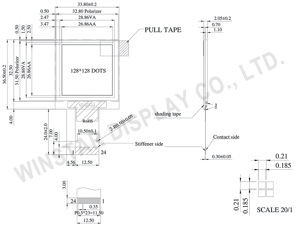
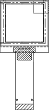
WEO128128A 是一款1.5吋單色被動式OLED顯示器模組,解析度為128x128 pixels。WEO128128A內建SSD1327 controller控制器, 支援多種傳輸介面: 6800 8-bite, 8080 8-bit 平行介面, I2C 與4線SPI串列介面。WEO128128A的模組尺寸為33.8 x 36.5 mm,AA區尺寸26.86 x 26.83 mm,3V驅動。WEO128128A為COG結構的OLED顯示器模組,為有機自發光,無須背光源,因此模組輕薄且低耗電流,此款WEO128128A模組非常適合手持式產品、量測儀器、物聯網裝置、工控設備等等。
此模組的工作溫度是-40℃至+80℃,儲存溫度-40℃至+80℃,如有產品需求或是需要更詳細資訊請與我們聯繫。
 可選 FPC
Data source ref: WEO128128ALAP3N00000
| 項目 | 尺寸 | 單位 |
|---|---|---|
| 點陣 | 128 x 128 Dots | - |
| 模組尺寸 | 33.80 x 36.50 x 2.05 | mm |
| 有效區域 | 26.86 x 26.86 | mm |
| 像素大小 | 0.185 x 0.185 | mm |
| 像素間距 | 0.210 x 0.210 | mm |
| 顯示模式 | 被動矩陣 | |
| 發光顏色 | 單色 | |
| 驅動方式 | 1/128Duty | |
| 灰階 | 4 bits | |
| IC | SSD1327 | |
| 介面 | 6800,8080,SPI,I2C | |
| 尺寸 | 1.5 吋 | |
| 參數 | 符號 | 最小值 | 最大值 | 單位 |
|---|---|---|---|---|
| 低壓電源,輸入/輸出 Pin 電源 | VCI | -0.3 | 4.0 | V |
| 邏輯電源電壓 | VDD | -0.5 | 2.75 | V |
| 顯示電源電壓 | VCC | -0.5 | 19.0 | V |
| 工作溫度 | TOP | -40 | +80 | °C |
| 儲存溫度 | TSTG | -40 | +85 | °C |
| 項目 | 符號 | 條件 | 最小值 | 典型值 | 最大值 | 單位 |
|---|---|---|---|---|---|---|
| 低壓電源,輸入/輸出 Pin 電源 | VCI | 2.8 | 3 | 3.3 | V | |
| 顯示電源電壓 | VCC | - | 14 | 14.5 | 15 | V |
| 邏輯電源電壓 | VDD | - | 2.4 | - | 2.6 | V |
| 輸入高準位 | VIH | - | 0.8×VCI | - | VCI | V |
| 輸入低準位 | VIL | - | 0 | - | 0.2×VCI | V |
| 輸出高準位 | VOH | - | 0.9×VCI | - | VCI | V |
| 輸出低準位 | VOL | - | 0 | - | 0.1×VCI | V |
| 50%顯示畫面耗電流 | VCC =14.5V | - | 24 | 36 | mA | |
| No. | 符號 | 功能說明 | ||||||||||
|---|---|---|---|---|---|---|---|---|---|---|---|---|
| 1 | VSS | Ground pin. It must be connected to external ground. | ||||||||||
| 2 | VCC | Power supply for panel driving voltage. This is also the most positive power voltage supply pin. It is supplied by external high voltage source. | ||||||||||
| 3 | VCOMH | COM signal deselected voltage level. A capacitor should be connected between this pin and VSS. No external power supply is allowed to connect to this pin. |
||||||||||
| 4 | VCI | Low voltage power supply and power supply for interface logic level. It should match with the MCU interface voltage level and must be connected to external source. VCI must always set to be equivalent to or higher than VDD. |
||||||||||
| 5 | VDD | Power supply pin for core logic operation. VDD can be supplied externally (within the range of 2.4V to 2.6V) or regulated Internally from VCI. A capacitor should be connected between VDD and VSS under all circumstances. |
||||||||||
| 6 | BS1 | MCU bus interface selection pins. Select appropriate logic setting as described in the following table. BS2 and BS1 are pin select. Bus Interface selection
|
||||||||||
| 7 | BS2 | |||||||||||
| 8 | VSS | Ground pin. It must be connected to external ground. | ||||||||||
| 9 | IREF | This pin is the segment output current reference pin | ||||||||||
| 10 | CS# | This pin is the chip select input connecting to the MCU. The chip is enabled for MCU communication only when CS# is pulled LOW (active LOW). |
||||||||||
| 11 | RES# | This pin is reset signal input. When the pin is pulled LOW, initialization of the chip is executed. Keep this pin pull HIGH during normal operation. |
||||||||||
| 12 | D/C | This pin is Data/Command control pin connecting to the MCU. When the pin is pulled HIGH, the data at D[7:0] will be interpreted as data. When the pin is pulled LOW, the data at D[7:0] will be transferred to a command register. In I2C mode, this pin acts as SA0 for slave address selection. |
||||||||||
| 13 | W/R# | This pin is read / write control input pin connecting to the MCU interface. When 6800 interface mode is selected, this pin will be used as Read/Write (R/W#) selection input. Read mode will be carried out when this pin is pulled HIGH and write mode when LOW. When 8080 interface mode is selected, this pin will be the Write (WR#) input. Data write operation is initiated when this pin is pulled LOW and the chip is selected. |
| 圖 | FPC 長度 | PIN | Pitch | ZIF FPC / HOTBAR FPC | 介面 | FPC No. | 建立日期 |
|---|---|---|---|---|---|---|---|
 |
25.05 | 24 | 0.5 | ZIF | 6800,8080,SPI,I2C | FPC2050002411XXXXX03 | 20150901 |
 |
41 | 24 | 0.5 | ZIF | 6800,8080,4-Wire SPI,I2C | FPC2050002411XXXXX12 | 20200116 |

通過點擊「允許所有 Cookie」,代表您同意在您的設備上存儲 Cookie 以增強網站瀏覽體驗、分析網站使用情況並協助我們的行銷和網站效能優化工作。您可以在我們的隱私權政策中找到有關於此的更多資訊。