

 - WF52ATLASDNT0")
 - 上視角 - WF52BTIASDNT0")
我們重視您的隱私
通過點擊「允許所有 Cookie」,代表您同意在您的設備上存儲 Cookie 以增強網站瀏覽體驗、分析網站使用情況並協助我們的行銷和網站效能優化工作。您可以在我們的隱私權政策中找到有關於此的更多資訊。


華凌光電的1.51吋OLED 透明顯示器模組設計旨在提供高可見度和優異的光學整合,並在緊湊且高效的包裝中實現。這是適用於需要清晰數據疊加而不遮擋背景的應用的理想解決方案。這款OLED 透明顯示器標準顏色為天藍色;但對於需要定制顏色選項,如白色、綠色、黃色、藍色和紅色,華凌可以根據需求提供量身定制的解決方案。
了解更多有關透明OLED顯示器(TOLED顯示器)的優勢與應用,並了解它如何革新光學儀器和即時數據疊加,請參閱我們的詳細指南。
| 項目 | 規格說明 | 單位 |
|---|---|---|
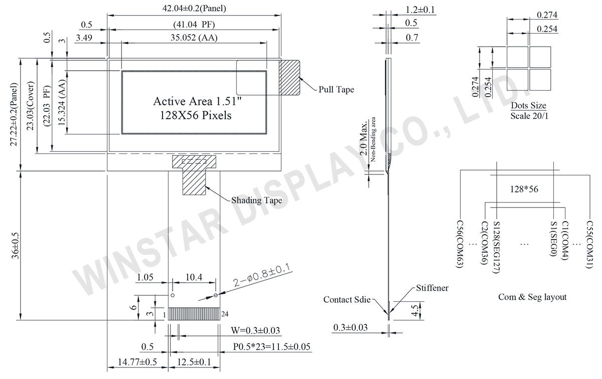
| 點陣(解析度) | 128 × 56 | - |
| 模組尺寸 | 42.04 × 27.22 × 1.2 | mm |
| 有效區域 | 35.052 × 15.324 | mm |
| 像素大小 | 0.254 × 0.254 | mm |
| 像素間距 | 0.274 × 0.274 | mm |
| 顯示模式 | Passive Matrix 被動矩陣 | |
| 顯示顏色 | 單色 | |
| 驅動方式 | 1/56 Duty | |
| IC | SSD1309 | |
| 介面 | 6800,8080,4線 SPI,I2C | |
| 尺寸 | 1.51吋 | |
| 參數 | 符號 | 最小值 | 最大值 | 單位 |
|---|---|---|---|---|
| 邏輯電源電壓 | VDD | -0.3 | 4 | V |
| 顯示電源電壓 | VCC | 0 | 17 | V |
| 工作溫度 | TOP | -40 | +80 | °C |
| 儲存溫度 | TSTG | -40 | +85 | °C |
| 項目 | 符號 | 條件 | 最小值 | 典型值 | 最大值 | 單位 |
|---|---|---|---|---|---|---|
| 邏輯電源電壓 | VDD | - | 1.65 | 3.0 | 3.3 | V |
| 顯示電源電壓 | VCC | - | 7.0 | 12.5 | 13.0 | V |
| 輸入高準位 | VIH | - | 0.8×VDD | - | - | V |
| 輸入低準位 | VIL | - | - | - | 0.2×VDD | V |
| 輸出高準位 | VOH | - | 0.9×VDD | - | - | V |
| 書出低準位 | VOL | - | - | - | 0.1×VDD | V |
| 顯示 50% 像素 | VCC =12.5V | - | 12 | 18 | mA | |
| No. | 符號 | 功能說明 | |||||||||||||||
|---|---|---|---|---|---|---|---|---|---|---|---|---|---|---|---|---|---|
| 1 | ESD_GND | ESD Ground pin. | |||||||||||||||
| 2 | VLSS | This is an analog ground pin | |||||||||||||||
| 3 | VSS | Ground. | |||||||||||||||
| 4 | NC | No connection | |||||||||||||||
| 5 | VDD | Power supply pin for core logic operation | |||||||||||||||
| 6 | BS1 | MCU bus interface selection pins. Select appropriate logic setting as described in the following table. BS2 and BS1 are pin select
(1) 0 is connected to VSS (2) 1 is connected to VDD |
|||||||||||||||
| 7 | BS2 | ||||||||||||||||
| 8 | CS# | This pin is the chip select input connecting to the MCU. The chip is enabled for MCU communication only when CS# is pulled LOW (active LOW). |
|||||||||||||||
| 9 | RES# | This pin is reset signal input. When the pin is pulled LOW, initialization of the chip is executed. Keep this pin pull HIGH during normal operation. |
|||||||||||||||
| 10 | D/C# | This pin is Data/Command control pin connecting to the MCU. When the pin is pulled HIGH, the data at D[7:0] will be interpreted as data. When the pin is pulled LOW, the data at D[7:0] will be transferred to a command register. In I2C mode, this pin acts as SA0 for slave address selection. |
|||||||||||||||
| 11 | R/W# | This pin is read / write control input pin connecting to the MCU interface. When 6800 interface mode is selected, this pin will be used as Read/Write (R/W#) selection input. Read mode will be carried out when this pin is pulled HIGH and write mode when LOW. When 8080 interface mode is selected, this pin will be the Write (WR#) input. Data write operation is initiated when this pin is pulled LOW and the chip is selected. When serial or I2C interface is selected, this pin must be connected to VSS. |
|||||||||||||||
| 12 | E/RD# | This pin is MCU interface input. When 6800 interface mode is selected, this pin will be used as the Enable (E) signal. Read/write operation is initiated when this pin is pulled HIGH and the chip is selected. When 8080 interface mode is selected, this pin receives the Read (RD#) signal. Read operation is initiated when this pin is pulled LOW and the chip is selected. When serial or I2C interface is selected, this pin must be connected to VSS. |
|||||||||||||||
| 13-20 | D0~D7 | These pins are bi-directional data bus connecting to the MCU data bus. Unused pins are recommended to tie LOW. When serial interface mode is selected, D0 will be the serial clock input: SCLK; D1 will be the serial data input: SDIN and D2 should be kept NC. When I2C mode is selected, D2, D1 should be tied together and serve as SDAout, SDAin in application and D0 is the serial clock input, SCL. |
|||||||||||||||
| 21 | IREF | This pin is the segment output current reference pin. IREF is supplied externally. A resistor should be connected between this pin and VSS to maintain the current around 10uA. |
|||||||||||||||
| 22 | VCOMH | COM signal deselected voltage level. A capacitor should be connected between this pin and VSS. |
|||||||||||||||
| 23 | VCC | Power supply for panel driving voltage. This is also the most positive power voltage supply pin. | |||||||||||||||
| 24 | ESD_GND | ESD Ground pin. |

通過點擊「允許所有 Cookie」,代表您同意在您的設備上存儲 Cookie 以增強網站瀏覽體驗、分析網站使用情況並協助我們的行銷和網站效能優化工作。您可以在我們的隱私權政策中找到有關於此的更多資訊。