 - WL0F00035000XGAAASA00")


 - WF104GSWAMLNN0")
私たちはあなたのプライバシーを大切にします
「すべてのクッキーを許可」をクリックすると、サイトのナビゲーションを向上させ、サイト使用状況を分析し、マーケティングおよびパフォーマンスの取り組みを支援するために、クッキーをデバイスに保存することに同意したことになります。この件に関する詳細情報は、ポリシーをご覧ください。プライバシーポリシー


WINSTARの1.51インチ透明OLEDディスプレイモジュールは、コンパクトで効率的なパッケージで高い視認性と優れた光学統合を提供するように設計されています。背景を遮ることなく明確なデータオーバーレイを必要とするアプリケーションに最適なソリューションです。この透明OLEDディスプレイは、標準色としてスカイブルーで提供されますが、ホワイト、グリーン、イエロー、ブルー、レッドなどのカスタマイズオプションもご要望に応じてWINSTARが提供できます。
有機EL透明 ディスプレイ(TOLEDディスプレイ)の利点とアプリケーションについての詳細は、光学機器やリアルタイムデータオーバーレイの革命的な使い方を含め、当社の詳細ガイドをご覧ください。
| 項目 | 仕様 | 単位 |
|---|---|---|
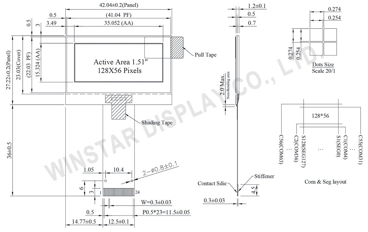
| ドットマトリックス(解像度) | 128 × 56 | - |
| モジュールサイズ | 42.04 × 27.22 × 1.2 | mm |
| 有効エリア | 35.052 × 15.324 | mm |
| ドットサイズ | 0.254 × 0.254 | mm |
| ドットピッチ | 0.274 × 0.274 | mm |
| 表示モード | パッシブマトリックス | |
| 発光色 | モノクロ | |
| 駆動方法 | 1/56 Duty | |
| IC | SSD1309 | |
| インターフェイス | 6800/8080/4-Wire SPI/I2C | |
| 表示サイズ(対角線) | 1.51 インチ | |
| パラメーター | 記号 | 最小値 | 最大値 | 単位 |
|---|---|---|---|---|
| ロジック電源電圧 | VDD | -0.3 | 4 | V |
| Display電源電圧 | VCC | 0 | 17 | V |
| 操作温度 | TOP | -40 | +80 | °C |
| 保存温度 | TSTG | -40 | +85 | °C |
| 項目 | 記号 | 条件 | 最小値 | 典型値 | 最大値 | 単位 |
|---|---|---|---|---|---|---|
| ロジック電源電圧 | VDD | - | 1.65 | 3.0 | 3.3 | V |
| Display電源電圧 | VCC | - | 7.0 | 12.5 | 13.0 | V |
| 高レベル入力 | VIH | - | 0.8×VDD | - | - | V |
| 低レベル入力 | VIL | - | - | - | 0.2×VDD | V |
| 高レベル出力 | VOH | - | 0.9×VDD | - | - | V |
| 低レベル出力 | VOL | - | - | - | 0.1×VDD | V |
| 50% チェックボード動作電流 | VCC =12.5V | - | 12 | 18 | mA | |
| No. | 記号 | 説明 | |||||||||||||||
|---|---|---|---|---|---|---|---|---|---|---|---|---|---|---|---|---|---|
| 1 | ESD_GND | ESD Ground pin. | |||||||||||||||
| 2 | VLSS | This is an analog ground pin | |||||||||||||||
| 3 | VSS | Ground. | |||||||||||||||
| 4 | NC | No connection | |||||||||||||||
| 5 | VDD | Power supply pin for core logic operation | |||||||||||||||
| 6 | BS1 | MCU bus interface selection pins. Select appropriate logic setting as described in the following table. BS2 and BS1 are pin select
(1) 0 is connected to VSS (2) 1 is connected to VDD |
|||||||||||||||
| 7 | BS2 | ||||||||||||||||
| 8 | CS# | This pin is the chip select input connecting to the MCU. The chip is enabled for MCU communication only when CS# is pulled LOW (active LOW). |
|||||||||||||||
| 9 | RES# | This pin is reset signal input. When the pin is pulled LOW, initialization of the chip is executed. Keep this pin pull HIGH during normal operation. |
|||||||||||||||
| 10 | D/C# | This pin is Data/Command control pin connecting to the MCU. When the pin is pulled HIGH, the data at D[7:0] will be interpreted as data. When the pin is pulled LOW, the data at D[7:0] will be transferred to a command register. In I2C mode, this pin acts as SA0 for slave address selection. |
|||||||||||||||
| 11 | R/W# | This pin is read / write control input pin connecting to the MCU interface. When 6800 interface mode is selected, this pin will be used as Read/Write (R/W#) selection input. Read mode will be carried out when this pin is pulled HIGH and write mode when LOW. When 8080 interface mode is selected, this pin will be the Write (WR#) input. Data write operation is initiated when this pin is pulled LOW and the chip is selected. When serial or I2C interface is selected, this pin must be connected to VSS. |
|||||||||||||||
| 12 | E/RD# | This pin is MCU interface input. When 6800 interface mode is selected, this pin will be used as the Enable (E) signal. Read/write operation is initiated when this pin is pulled HIGH and the chip is selected. When 8080 interface mode is selected, this pin receives the Read (RD#) signal. Read operation is initiated when this pin is pulled LOW and the chip is selected. When serial or I2C interface is selected, this pin must be connected to VSS. |
|||||||||||||||
| 13-20 | D0~D7 | These pins are bi-directional data bus connecting to the MCU data bus. Unused pins are recommended to tie LOW. When serial interface mode is selected, D0 will be the serial clock input: SCLK; D1 will be the serial data input: SDIN and D2 should be kept NC. When I2C mode is selected, D2, D1 should be tied together and serve as SDAout, SDAin in application and D0 is the serial clock input, SCL. |
|||||||||||||||
| 21 | IREF | This pin is the segment output current reference pin. IREF is supplied externally. A resistor should be connected between this pin and VSS to maintain the current around 10uA. |
|||||||||||||||
| 22 | VCOMH | COM signal deselected voltage level. A capacitor should be connected between this pin and VSS. |
|||||||||||||||
| 23 | VCC | Power supply for panel driving voltage. This is also the most positive power voltage supply pin. | |||||||||||||||
| 24 | ESD_GND | ESD Ground pin. |

「すべてのクッキーを許可」をクリックすると、サイトのナビゲーションを向上させ、サイト使用状況を分析し、マーケティングおよびパフォーマンスの取り組みを支援するために、クッキーをデバイスに保存することに同意したことになります。この件に関する詳細情報は、ポリシーをご覧ください。プライバシーポリシー