

私たちはあなたのプライバシーを大切にします
「すべてのクッキーを許可」をクリックすると、サイトのナビゲーションを向上させ、サイト使用状況を分析し、マーケティングおよびパフォーマンスの取り組みを支援するために、クッキーをデバイスに保存することに同意したことになります。この件に関する詳細情報は、ポリシーをご覧ください。プライバシーポリシー


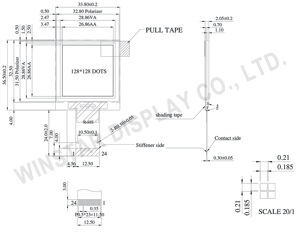
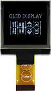
WEO128128Aは128×128ピクセルで構成される対角寸法1.5インチのパッシブマトリックスOLEDディスプレイです。WEO128128Aの外観寸法が33.8 x 36.5 mm、AAサイズが26.86 x 26.83 mmです。それはSSD1327コントローラICで内蔵されており、6800/8080の8ビットパラレル、I2C及び4線式SPIシリアルインタフェース、3V電源を介して通信されます。WEO128128Aは超薄いCOG構造する有機ELディスプレイ、それにバックライトが不要(自己発光)ですので、軽量、低消費電力です。この有機ELモジュールはハンドヘルド機器、メーター、IoT、ETC車載器等のアイテムに適しています。
WEO128128Aの操作温度は -40℃ ~ +80℃、保存温度は-40℃ ~ +80℃です。下記にWEO128128Aの基本的な仕様です。サンプルやより詳細な情報については、当社の営業担当者にお問い合わせください
 FPC Options
Data source ref: WEO128128ALAP3N00000
| 項目 | 仕様 | 単位 |
|---|---|---|
| ドットマトリックス | 128 x 128 Dots | - |
| モジュールサイズ | 33.80 x 36.50 x 2.05 | mm |
| アクティブエリア | 26.86 x 26.86 | mm |
| ピクセルサイズ | 0.185 x 0.185 | mm |
| ピクセルピッチ | 0.210 x 0.210 | mm |
| 表示モード | パッシブマトリクス | |
| 発光色 | モノクロ | |
| 駆動方法 | 1/128 Duty | |
| グレースケール | 4 bits | |
| IC | SSD1327 | |
| インターフェイス | 6800,8080,SPI,I2C | |
| サイズ | 1.5インチ | |
| パラメーター | 條件 | 最小値 | 最大値 | 単位 |
|---|---|---|---|---|
| 低電圧電源, 入力/出力ピンの電源電圧 | VCI | -0.3 | 4.0 | V |
| ロジック電源電圧 | VDD | -0.5 | 2.75 | V |
| 表示用電源電圧 | VCC | -0.5 | 19.0 | V |
| 動作温度 | TOP | -40 | +80 | °C |
| 保存温度 | TSTG | -40 | +85 | °C |
| 項目 | 條件 | 条件 | 最小値 | 典型値 | 最大値 | 単位 |
|---|---|---|---|---|---|---|
| 低電圧電源, 入力/出力ピンの電源電圧 | VCI | 2.8 | 3 | 3.3 | V | |
| 表示用電源電圧 | VCC | - | 14 | 14.5 | 15 | V |
| ロジック電源電圧 | VDD | - | 2.4 | - | 2.6 | V |
| 高レベル入力 | VIH | - | 0.8×VCI | - | VCI | V |
| 低レベル入力 | VIL | - | 0 | - | 0.2×VCI | V |
| 高レベル出力 | VOH | - | 0.9×VCI | - | VCI | V |
| 低レベル出力 | VOL | - | 0 | - | 0.1×VCI | V |
| 50% Check Board operating Current | VCC =14.5V | - | 24 | 36 | mA | |
| No. | 記号 | 説明 | ||||||||||
|---|---|---|---|---|---|---|---|---|---|---|---|---|
| 1 | VSS | Ground pin. It must be connected to external ground. | ||||||||||
| 2 | VCC | Power supply for panel driving voltage. This is also the most positive power voltage supply pin. It is supplied by external high voltage source. | ||||||||||
| 3 | VCOMH | COM signal deselected voltage level. A capacitor should be connected between this pin and VSS. No external power supply is allowed to connect to this pin. |
||||||||||
| 4 | VCI | Low voltage power supply and power supply for interface logic level. It should match with the MCU interface voltage level and must be connected to external source. VCI must always set to be equivalent to or higher than VDD. |
||||||||||
| 5 | VDD | Power supply pin for core logic operation. VDD can be supplied externally (within the range of 2.4V to 2.6V) or regulated Internally from VCI. A capacitor should be connected between VDD and VSS under all circumstances. |
||||||||||
| 6 | BS1 | MCU bus interface selection pins. Select appropriate logic setting as described in the following table. BS2 and BS1 are pin select. Bus Interface selection
|
||||||||||
| 7 | BS2 | |||||||||||
| 8 | VSS | Ground pin. It must be connected to external ground. | ||||||||||
| 9 | IREF | This pin is the segment output current reference pin | ||||||||||
| 10 | CS# | This pin is the chip select input connecting to the MCU. The chip is enabled for MCU communication only when CS# is pulled LOW (active LOW). |
||||||||||
| 11 | RES# | This pin is reset signal input. When the pin is pulled LOW, initialization of the chip is executed. Keep this pin pull HIGH during normal operation. |
||||||||||
| 12 | D/C | This pin is Data/Command control pin connecting to the MCU. When the pin is pulled HIGH, the data at D[7:0] will be interpreted as data. When the pin is pulled LOW, the data at D[7:0] will be transferred to a command register. In I2C mode, this pin acts as SA0 for slave address selection. |
||||||||||
| 13 | W/R# | This pin is read / write control input pin connecting to the MCU interface. When 6800 interface mode is selected, this pin will be used as Read/Write (R/W#) selection input. Read mode will be carried out when this pin is pulled HIGH and write mode when LOW. When 8080 interface mode is selected, this pin will be the Write (WR#) input. Data write operation is initiated when this pin is pulled LOW and the chip is selected. |
| 写真 | FPC Length | PIN | Pitch | ZIF FPC or HOTBAR FPC | インターフェイス | FPC No. | Create Date |
|---|---|---|---|---|---|---|---|
 |
25.05 | 24 | 0.5 | ZIF | 6800,8080,SPI,I2C | FPC2050002411XXXXX03 | 20150901 |
 |
41 | 24 | 0.5 | ZIF | 6800,8080,4-Wire SPI,I2C | FPC2050002411XXXXX12 | 20200116 |

「すべてのクッキーを許可」をクリックすると、サイトのナビゲーションを向上させ、サイト使用状況を分析し、マーケティングおよびパフォーマンスの取り組みを支援するために、クッキーをデバイスに保存することに同意したことになります。この件に関する詳細情報は、ポリシーをご覧ください。プライバシーポリシー